Bootstrapped and correlated double sampling (BCDS) non-contact touch sensor for mobile devices

a non-contact, double-sampling technology, applied in pulse generation, logic circuits, instruments, etc., can solve the problems of limited battery and space resources, infused into space and battery constrained mobile devices, tablets and smartphones, etc., to achieve accurate determination of position (motion), increase accuracy and noise-immunity

Active Publication Date: 2018-10-23
RGT UNIV OF CALIFORNIA
View PDF28 Cites 2 Cited by
  • Summary
  • Abstract
  • Description
  • Claims
  • Application Information

AI Technical Summary

Benefits of technology

[0012]The present technology uses an oscillator, counter and a count storage and comparison circuit to more accurately determine the position (motion) of a finger hovering over the display of a portable electronic device, such as a Smartphone. Any portable electronic device with a display can incorporate this technology to provide a 2D or 3D non-contact interface.
[0013]Unlike capacitive sensing, using an oscillator provides much higher gain and allows the device to be more sensitive to the position and movement of the user's finger over the touchscreen. This bootstrapping and correlated double sampling (BCDS) sensing apparatus uses a double sampling approach, in which the oscillator first senses the active channel and then senses the reference channel and by subtracting these two results from one another a correlated output is generated. In combination with this is a calibration sequence which assures all channels have the same loading, and bootstrapping which eliminates the effect of loading between channels. By performing the calibration and bootstrapping interoperably with the double sampling technique measurement accuracy is significantly improved. In addition, as a result of these interoperative enhancements, the present technology provides reduced sensitivity to noises, both external and electronic, far beyond what is possible with a conventional electrostatic capacitive sensor.

Problems solved by technology

While significant progress has been made in developing 3D contactless touch sensors for larger television and monitor type displays, it has yet to be infused into space and battery constrained mobile devices (i.e., tablets and smartphones).
In addition, any successful 3D sensing solution for mobile devices must consume low power and small silicon area to be compatible with limited battery and space resources.

Method used


Image

  • Bootstrapped and correlated double sampling (BCDS) non-contact touch sensor for mobile devices
  • Bootstrapped and correlated double sampling (BCDS) non-contact touch sensor for mobile devices
  • Bootstrapped and correlated double sampling (BCDS) non-contact touch sensor for mobile devices

Examples


embodiment 70

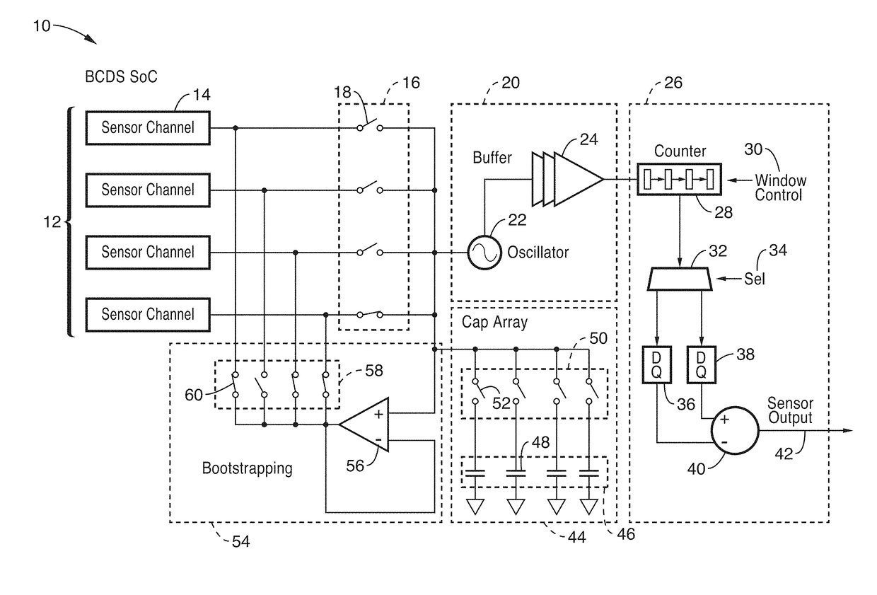
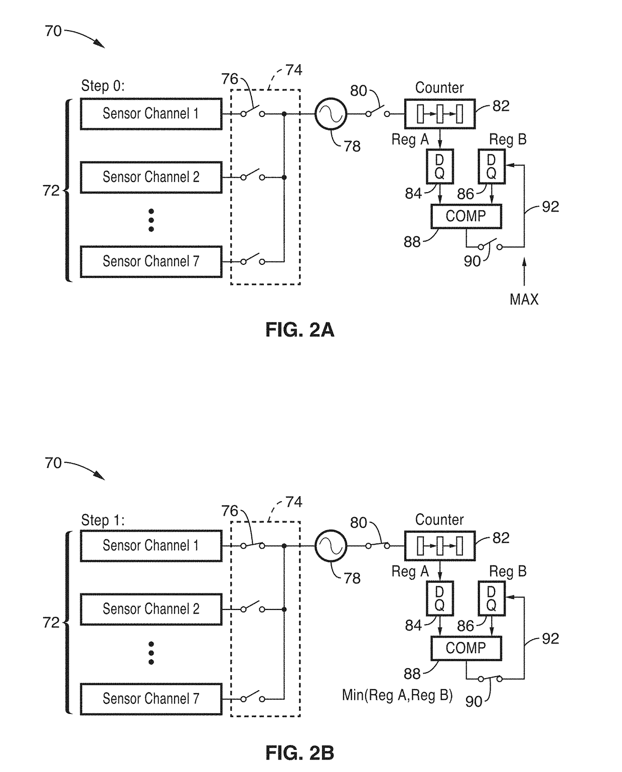
[0045]FIG. 2A through FIG. 2D and FIG. 3A through FIG. 3D illustrate an embodiment 70 in which the highest load for the channels is determined (FIG. 2A-FIG. 2D) and then the capacitance of each sensing channel is calibrated (FIG. 3A-FIG. 3D) to a reference value using a capacitor array based on a successive approximation register (SAR) principles (runs on startup) toward achieving high sampling accuracy.

[0046]During each measurement cycle, the oscillator is first connected to the desired input channel for a given integration time (programmable from 0.1 ms to 100 ms), such as was seen in FIGS. 2A-2D, and then connected to a reference channel with identical capacitance (calibrated by the capacitor array during initialization) for the same integration window, as seen in FIG. 3A-3D.

[0047]In FIG. 2A through FIG. 2D an embodiment 70 is illustrated in which each of multiple sensor channels 72 can be coupled through multiple switches 74 to the oscillator 78, each switch 76 allowing individu...

embodiment 190

[0057]FIG. 5 through FIG. 7 illustrate elements of a bootstrap circuit embodiment 190 for eliminating the capacitance between input electrode channels of the touch screen. In FIG. 5 an example embodiment 190 of a boot circuit is shown with active channel 192, with its capacitive load 194, coupled to oscillator 196 and buffered by an amplifier 200. Also seen in the figure is the inter-channel capacitance 198 (between input channels) which arises between the active channel and inactive channels 202. As the electrode array is scanned, a unity-gain amplifier 200 is used to sense the time-domain voltage of the active channel and replicate it on the remaining idle channels to nullify the coupling capacitance by enforcing equal potential across the inter-channel coupling capacitors.

[0058]In FIG. 6 an example embodiment for a unity gain amplifier circuit 200 is shown with two current paths through transistors 202a, 202b, in totem-pole configuration with transistors 204a, 204b gated by diffe...

embodiment 290

[0080]FIG. 16 illustrates an embodiment 290 of a touch sensing device, having a housing 292, and display 294, about which are placed multiple detectors. In the example shown, one each of detectors 296a, 296b, 296c, 296d are placed at each of the four corners of the touch screen display of a portable electronic device for position detection. Using this configuration, the counts of the four detectors can be compared to estimate the location of a finger over the display surface. Although sensor inputs are shown for the sake of simplicity being separate from the display, it should be appreciated that for this embodiment and others described herein, that the sensor channels can be incorporated into the display itself, and may comprise a plurality of sensors, for instance greater than sixteen, and up to dozens of sensor channels.

[0081]FIG. 17 depicts a timing diagram for the signals seen in FIG. 15, showing the Dicke switch signal, counter trigger signal, and oscillator signal. A test cir...


PUM


Abstract

Non-contact position and motion sensing is improved for oscillator frequency based sensors in response to adding a two phase calibration along with bootstrapping circuit. Calibration is performed across the multiple sensor channels, so that: (1) maximum sensor channel loading is determined, and (2) the amount of capacitive load required for each other channel to match this same maximum load is stored for application to that channel during non-contact sensing. Capacitive coupling between channels is nullified by a bootstrapping process, in which time-domain voltage on the active channel is replicated on the non-active channels during non-contact sensing, thus creating equal potentials across inter-channel couplings that effectively eliminate inter-channel capacitive loading.

Description

CROSS-REFERENCE TO RELATED APPLICATIONS[0001]This application is a 35 U.S.C. § 111(a) continuation of PCT international application number PCT / US2015 / 020577 filed on Mar. 13, 2015, incorporated herein by reference in its entirety, which claims priority to, and the benefit of U.S. provisional patent application Ser. No. 61 / 953,004 filed on Mar. 14, 2014, incorporated herein by reference in its entirety, and which also claims priority to, and the benefit of and U.S. provisional patent application Ser. No. 62 / 067,968 filed on Oct. 23, 2014, incorporated herein by reference in its entirety. Priority is claimed to each of the foregoing applications.[0002]The above-referenced PCT international application was published as PCT International Publication No. WO 2015 / 138984 on Sep. 17, 2015, which publication is incorporated herein by reference in its entirety.STATEMENT REGARDING FEDERALLY SPONSORED RESEARCH OR DEVELOPMENT[0003]Not ApplicableINCORPORATION-BY-REFERENCE OF COMPUTER PROGRAM APPE...

Claims


Application Information

Patent Timeline
Patent Type & Authority Patents(United States)
IPC IPC(8): G06F3/044H03K3/03H03K17/955G06F3/041
CPCG06F3/0418G06F3/044H03K3/0315H03K17/955H03K2217/960715G06F2203/04101G06F2203/04108H03K2217/94026G06F3/04182
Inventor TANG, ADRIAN J.CHANG, MAU-CHUNG FRANK
Owner RGT UNIV OF CALIFORNIA
Why Eureka
Try Eureka