Extended voltage range coldspare tolerant off chip driver

a technology of off-chip drivers and extended voltage range, which is applied in the direction of logic circuit coupling/interface arrangement, power consumption reduction, pulse technique, etc., can solve the problems of continuing need and continuing problems with off-chip drivers and their cold spare capabilities, and achieve the effect of preventing a build-up of voltage over time and prolonging the voltage rang

Active Publication Date: 2018-11-20
BAE SYST INFORMATION & ELECTRONICS SYST INTERGRATION INC
View PDF14 Cites 9 Cited by
  • Summary
  • Abstract
  • Description
  • Claims
  • Application Information

AI Technical Summary

Benefits of technology

[0007]In one aspect, an exemplary embodiment the present disclosure may provide an off chip driver circuit comprising: a functional mode at a first voltage; and a cold spare mode at the first voltage; wherein the circuit supports the first voltage in both the functional mode and the cold spare mode. This embodiment or another embodiment may further include a bias circuit; and an off chip driver sub-cell circuit, wherein the bias circuit is operatively coupled to the off chip driver sub-cell circuit and the bias circuit generates signals for cold spare voltage protection in the off chip driver. This embodiment or another embodiment may further include a chip pad input / output (I / O) having a signal to be protected pass therethrough; a first diode in electrical communication with the chip pad I / O; a second diode in series with the first diode; wherein the first and second diodes define a feedback voltage in an electro static discharge (ESD) device with the chip pad i / o to cause the circuit to be transparent in functional mode and operational in cold spare mode. This embodiment or another embodiment may further include a first output (vir_vdd_io); a second output (vir_vbias); wherein the first output (vir_vdd_io) and second output (vir_vbias) are operatively connected to the off chip driver sub-cell circuit; wherein when the bias circuit is in the functional mode, the first output (vir_vdd_io) equals a driver circuit power supply voltage (vdd_io) such that the first and second diodes are electrically transparent such that signals flow directly and uninterrupted from the driver circuit power supply voltage (vdd_io) to first output (vir_vdd_io). This embodiment or another embodiment may further include a first p-channel field effect transistor (pFET) electrically coupled between the first output (vir_vdd_io) and the driver circuit power supply voltage (vdd_io) configured to be turned off in cold spare mode to pass voltage directly from the driver circuit power supply voltage (vdd_io) to the first output (vir_vdd_io). This embodiment or another embodiment may further include wherein the first and second diodes siphons input voltage from the chip pad i / o in the cold spare mode. This embodiment or another embodiment may further include wherein subtracting the second voltage from the first voltage is adapted to enable transistors to be stacked to support the similar voltage in the cold spare mode. This embodiment or another embodiment may further include a bias voltage generated from the driver circuit power supply voltage (vdd_io) in functional mode and generated from the two series diodes in the ESD in cold spare mode, wherein the bias voltage is adapted to maintain other transistors below an operating voltage maximum for each of the other transistors while the total circuit operates at higher than the voltage maximum for each respective transistor. This embodiment or another embodiment may further include an off-state and an on-state of the first and second diodes; a threshold voltage of the first and second diodes, wherein when voltage from the chip pad I / O exceeds the threshold voltage, the first and second diodes are switched from the off-state to the on-state, and switching the first and second diodes from the off-state to the on-state switches the circuit from the functional mode to the cold spare mode. This embodiment or another embodiment may further include wherein when the bias circuit is in cold spare mode, the voltage at the first output (vir_vdd_io) is two diode drops less than the voltage at the first output (vir_vdd_io) in functional mode, and the voltage at the second output (vir_vbias) is two diode drops less than the voltage at the second output (vir_vbias) in functional mode. This embodiment or another embodiment may further include wherein the bias circuit does not affect functionality of the off chip driver sub-cell circuit in functional mode. This embodiment or another embodiment may further include at least one resistor located intermediate the first input (vdd_io) and the first output (vir-vdd_io) to bleed voltage prior to the first output in the cold spare mode adapted to assist phantom powering of the first output (vir_vdd_io) in cold spare mode to prevent a build up of voltage over time. This embodiment or another embodiment may further include a functional mode first voltage and the first input (vdd_io); a functional mode second voltage at a second input (vbias); wherein the functional mode first and second voltages at the respective first and second inputs are different. This embodiment or another embodiment may further include a first inverter having a first inverter input; a second inverter having a second inverter input; wherein the first and second inverters include stacked transistors adapted to operate at an extended voltage range. This embodiment or another embodiment may further include wherein the first and second inverter inputs receive one signal therethrough at different voltage levels, and the signal is sent through the first and second inverters to the chip pad I / O. This embodiment or another embodiment may further include wherein if the circuit is powered off and in the cold spare mode, any voltage applied to the chip pad io is sent through the first and second diodes and out through the first output (vir_vdd_io) and the second output (vir_vbias) and into respective vir_vdd_io and vir_vbias inputs in the off chip driver circuit.
[0008]In another aspect, an embodiment of the present disclosure may provide a method comprising: providing an off chip driver circuit that switches between a functional mode and a cold spare mode, wherein the off chip driver circuit supports similar voltage in both the functional mode and the cold spare mode; passing supply and voltage protection signals through a bias circuit in the off chip drive circuit in the functional mode but passing voltages derived from a chip pad in the cold spare mode; and receiving the voltage signals, in an off chip driver sub-circuit, from the off bias circuit. This embodiment may further provide inputting a first voltage at a first input (vdd_io) and sending the first voltage towards a first output (vir_vdd_io); subtracting a second voltage passing through at least two diodes from the first voltage from the first voltage to establish a third voltage; and outputting the third voltage through the first output; wherein subtracting the second voltage from the first voltage is adapted to enable transistors to be stacked to support the similar voltage in the cold spare mode. This embodiment or another embodiment may further include creating bias voltages by sending voltage through two series diodes; applying the bias voltages to other transistors in the circuit, which is adapted to maintain the other transistors below an operating voltage maximum for each of the other transistors. This embodiment or another embodiment may further include in functional mode, generating the bias voltages directly from the first input (vdd_io); and in cold spare mode, generating the bias voltages through two series diodes coupled with a chip pad input / output (I / O). This embodiment or another embodiment may further include switching the two series diodes from and off-state to an on-state when voltage across the two series diodes exceeds a threshold voltage; and wherein switching the two series diodes from the off-state to the on-state switches the circuit from the functional mode to the cold spare mode. This embodiment or another embodiment may further include bleeding voltage into the first output (vir_vdd_io) across the two series diodes from a chip pad input / output (I / O) in cold spare mode; precluding voltage from bleeding voltage into the first output (I / O) so as to be functionally transparent in the functional mode. This embodiment or another embodiment may further include passing voltage from the first input to the first output without any effect from the two series diodes in functional mode; and passing voltage from a second input (vbias) to a second output (vir_vbias) without any effect from the two series diodes in functional mode.

Problems solved by technology

The second reason, is that many times there may be redundant computer cards that are physically powered off until they are needed when the first one fails.
Issues continue to exist with off chip drivers and their cold spare capabilities.
One of the issues is a need continues for an off chip driver with cold spare capability that is able to handle a similar voltage in both the functional mode and a cold spare mode.

Method used


Image

  • Extended voltage range coldspare tolerant off chip driver
  • Extended voltage range coldspare tolerant off chip driver
  • Extended voltage range coldspare tolerant off chip driver

Examples


Embodiment Construction

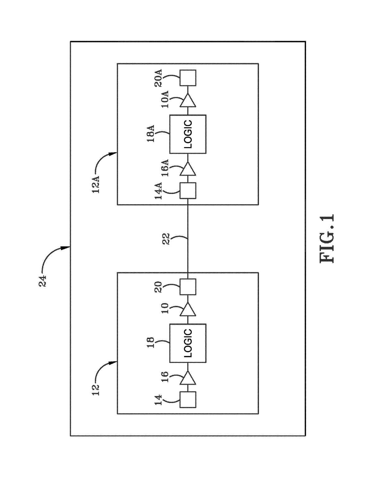
[0022]An off chip driver in accordance with one aspect of the present disclosure is shown generally throughout the figures at 10. The off chip driver 10 is part of an integrated circuit chip 12, which may also be referred to as a first chip 12 including an input / output (I / O) pad 14 connected with an on chip receiver 16 connected with logic 18 which is connected with the off chip driver 10 which is connected with the input / output pad 20. First chip 12 may be connected with a second chip 12A having similar components as the first chip 12. Similar components of second chip 12A are designated with the letter “A” after the respective reference numeral. I / O pad 14A on second chip 12A is an electrical communication with I / O pad 20 of chip 12 via line 22. The first and second chips 12, 12A are supported by a card 24 which is configured to be integrated into a computer or other electrical circuitry as one having ordinary skill in the art would understand.

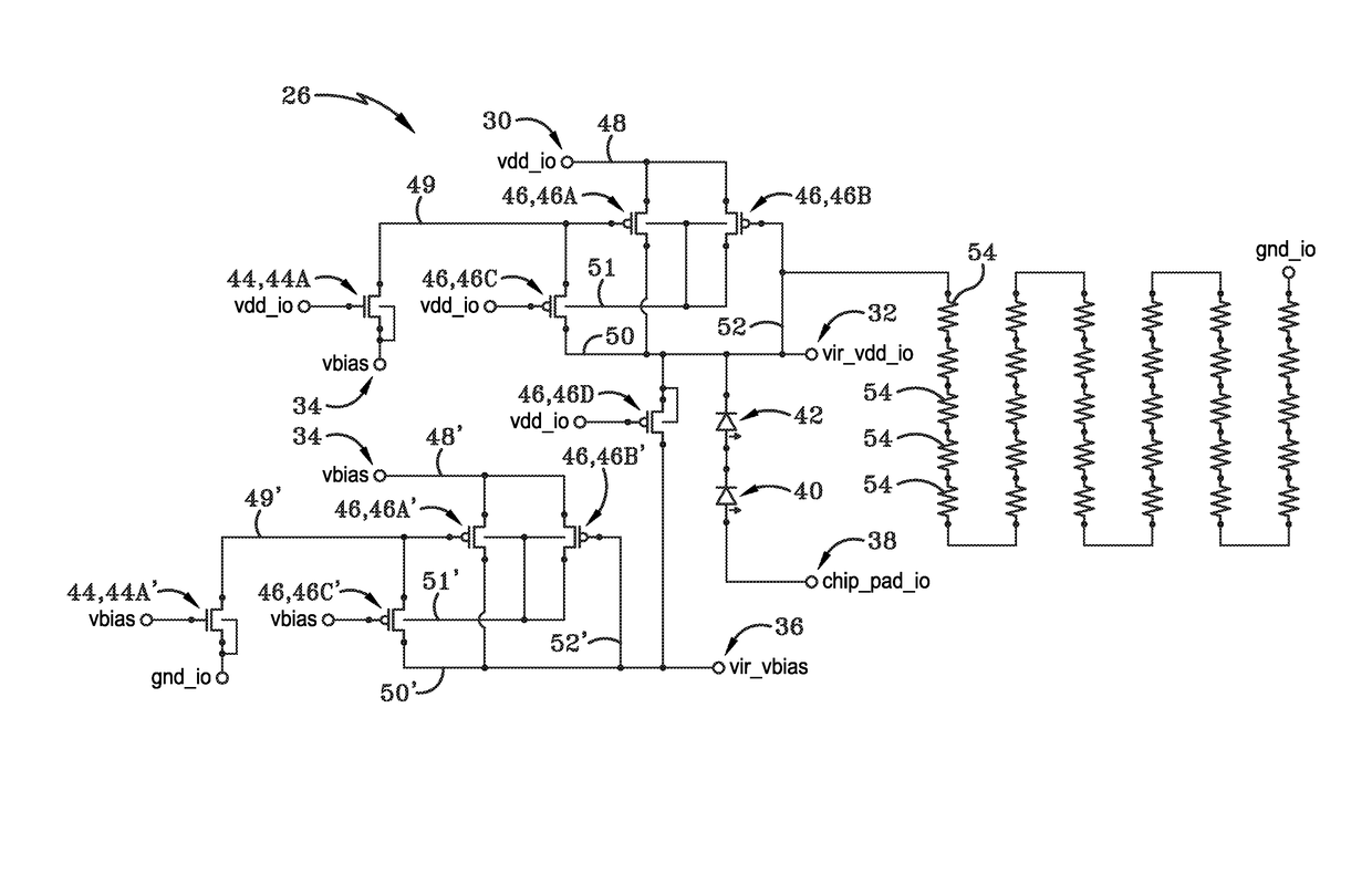
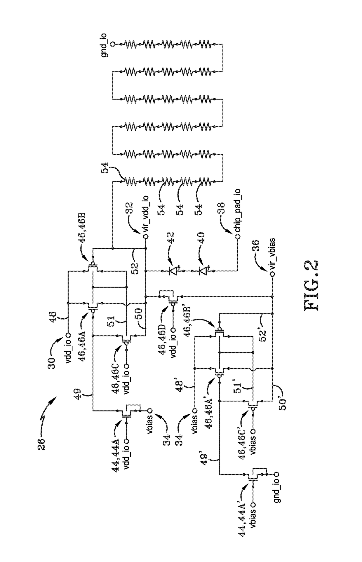
[0023]The off chip driver 10 includes...


PUM


Abstract

An off chip driver circuit includes a bias circuit and a driver sub-cell circuit. The bias circuit and off chip driver sub-cell circuit are in electrical communication with each other. The bias circuit includes two serially aligned diodes which are in an off-state when the driver sub-cell is in a functional mode and which are in an on-state when the driver sub-cell is in a cold spare mode. The arrangement of the diodes enables the off chip driver circuit to handle similar voltage signals in both the functional mode and the cold spare mode.

Description

BACKGROUNDTechnical Field[0001]The present disclosure relates to circuits having cold spare capabilities. More particularly, the present disclosure relates to an off chip driver with an extended voltage range in a cold spare mode.Background Information[0002]An off chip driver circuit typically drives logic levels relating to supply voltages of the circuit off the chip while protecting against any high voltages which may occur when the off chip driver circuit is disabled and its output terminal is coupled to an external circuit operating at a higher supply voltage. It is desirable to provide this protection while minimizing the number of transistors and therefore the chip area utilized by the off chip driver circuit. Off chip drivers include electronic circuitry which is configured to send at least one signal from one chip to another chip, as the at least one signal is being driven off the chip, hence the name “off chip driver.” Off chip driver circuits are commonly used to allow suc...

Claims


Application Information

Patent Timeline
Patent Type & Authority Patents(United States)
IPC IPC(8): H03K19/003H03K19/177H03K19/00H03K19/0185H03K17/0814
CPCH03K19/00315H03K19/17744H03K19/0016H03K19/01855H03K19/17788H03K17/08142
Inventor ROSS, JASON F.
Owner BAE SYST INFORMATION & ELECTRONICS SYST INTERGRATION INC
Why Eureka
Try Eureka