Method for producing wired circuit board

a wired circuit board and wire technology, applied in the field of wired circuit board production, can solve the problem that the wiring pattern cannot be prevented and the wiring pattern is not adequate, and achieve the effect of excellent connection reliability and reduced light projected toward the above-described portion

Active Publication Date: 2018-11-27
NITTO DENKO CORP
View PDF19 Cites 4 Cited by
  • Summary
  • Abstract
  • Description
  • Claims
  • Application Information

AI Technical Summary

Benefits of technology

[0010]The present invention provides a method for producing a wired circuit board by which a conductive pattern can be provided more freely and inadequate formation of conductive pattern can be suppressed.
[0022]With the method for producing a wired circuit board of the present invention, a wired circuit board with excellent connection reliability can be produced.

Problems solved by technology

Then, there are disadvantages in that inadequate formation of the wiring pattern cannot be prevented.

Method used


Image

  • Method for producing wired circuit board
  • Method for producing wired circuit board
  • Method for producing wired circuit board

Examples


first embodiment

1. First Embodiment

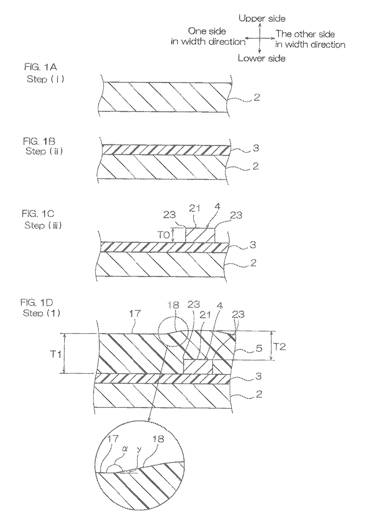
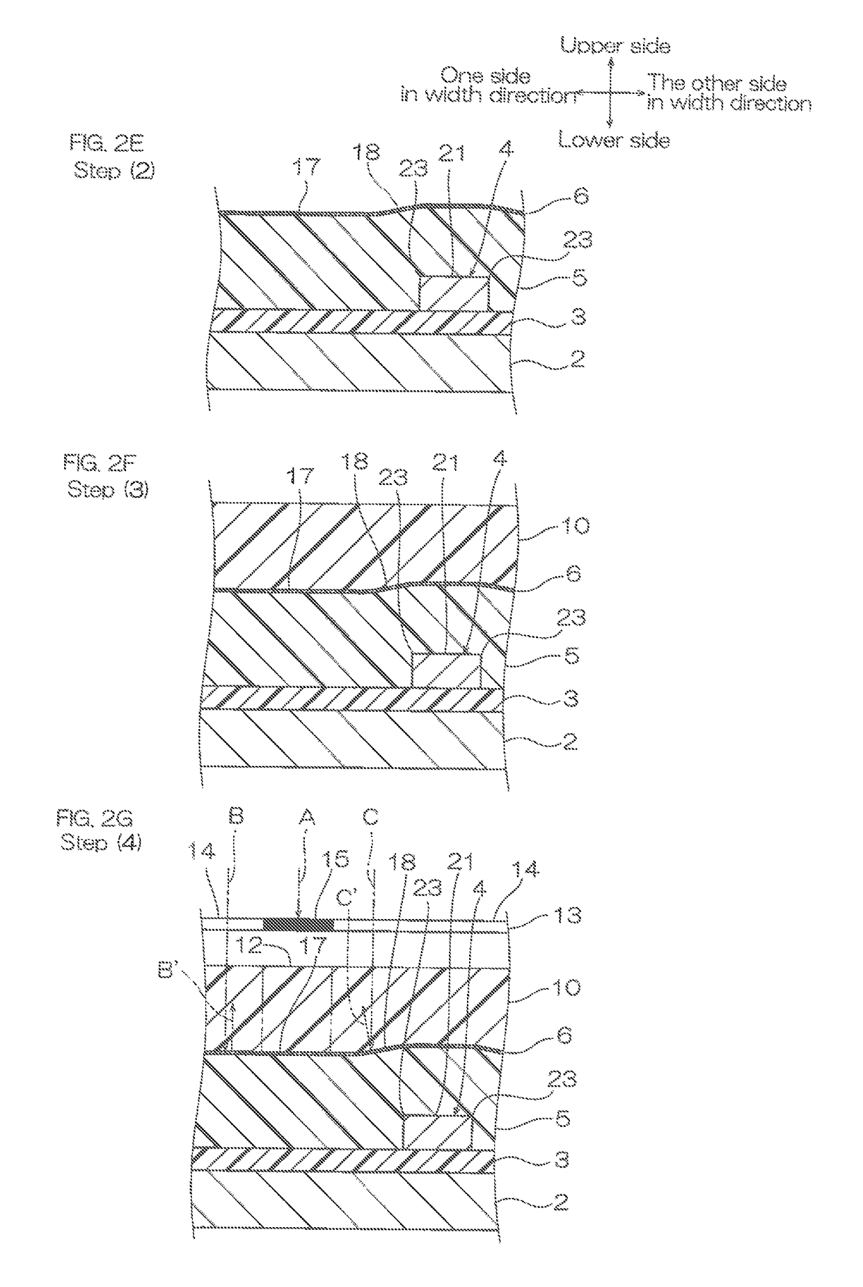
[0062]The method for producing a suspension board with circuits 1 includes a step (i) (ref: FIG. 1A) in which a metal supporting board 2 is prepared, a step (ii) (ref: FIG. 1B) in which an insulating base layer 3 is provided on the metal supporting board 2, a step (iii) (ref: FIG. 1C) in which a first conductive pattern 4 is provided on the insulating base layer 3, and a step (1) (ref: FIG. 1D) in which an intermediate insulating layer 5 as an example of the insulating layer is provided on the insulating base layer 3 so as to cover the first conductive pattern 4. The method for producing a suspension board with circuits 1 also includes a step (2) (ref: FIG. 2E) in which a metal thin film 6 is provided on at least an inclined face 18 of the intermediate insulating layer 5, a step (3) (ref: FIG. 2F) in which a photoresist 10 is provided on the metal thin film 6, and a step (4) (ref: FIG. 2G and FIG. 6A) in which a photomask 13 is disposed so that a to-be-portion 12 ...

second embodiment

2. Second Embodiment

[0150]In the second embodiment, for those members and steps as those in the first embodiment, the same reference numerals are given and detailed descriptions thereof are omitted.

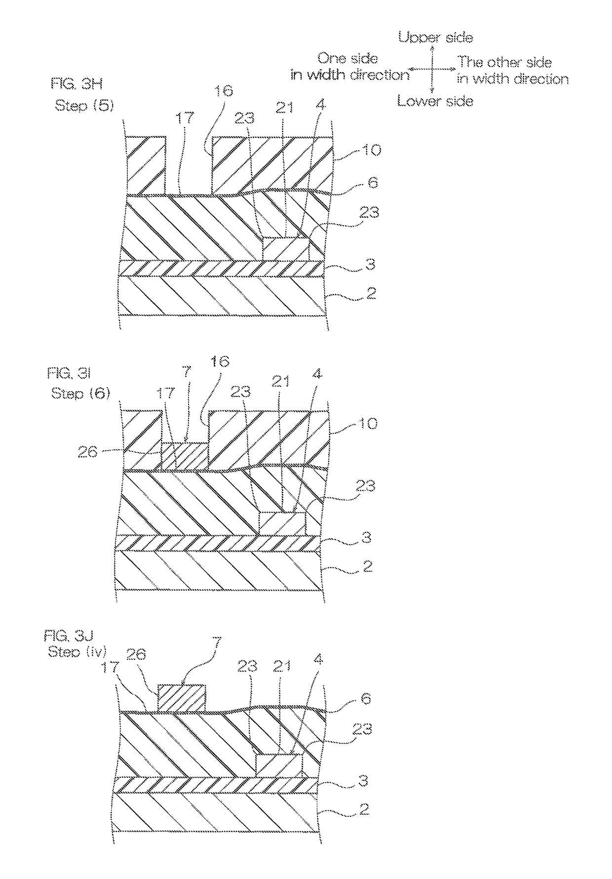
[0151]Production method in the second embodiment further includes, in addition to the steps in the production method of the first embodiment, as shown in FIG. 9A and FIG. 9B, a step (7) in which at least the inclined face 18 is roughened.

[0152]The step (7) is performed after the step (1), in which the intermediate insulating layer 5 is provided, and before the step (2), in which the metal thin film 6 is provided. That is, in the second embodiment, the step (i) to step (1), step (7), and step (2) to step (vi) are performed sequentially.

[0153]That is, in this method, with the step (i) to step (1), the metal supporting board 2, insulating base layer 3, first conductive pattern 4, and intermediate insulating layer 5 are provided.

[0154]Meanwhile, in the second embodiment, in the step (1), the ...

third embodiment

3. Third Embodiment

[0165]In the third embodiment, for the same members and the steps as in the first embodiment and the second embodiment, the same reference numerals are given and detailed descriptions thereof are omitted.

[0166]The production method of the third embodiment further includes, in addition to the steps in the production method of the first embodiment, a step (8), in which the metal thin film 6 is allowed to have a reflectivity for light having a wavelength of 365 nm of 25% or less.

[0167]The step (8) is performed, after the step (2) and before the step (3). That is, in the third embodiment, step (i) to step (2), step (8), and step (3) to step (vi) are performed sequentially.

[0168]That is, in this method, with the step (i) to step (2), the metal supporting board 2, insulating base layer 3, first conductive pattern 4, intermediate insulating layer 5, and metal thin film 6 are provided, respectively.

[0169]Meanwhile, in the third embodiment, in the step (1), the supplementa...


PUM

PropertyMeasurementUnit
angleaaaaaaaaaa
angleaaaaaaaaaa
distanceaaaaaaaaaa

Abstract

The method for producing a wired circuit board including an insulating layer and a conductive pattern provided on the insulating layer includes the steps of the following: a step (1), in which the insulating layer is provided; a step (2), in which a metal thin film is provided on an inclined face of the insulating layer; a step (3), in which a photoresist is provided on the metal thin film; a step (4), in which a photomask is disposed so that in the photoresist, a portion where the conductive pattern is to be provided is shielded from light, and the photoresist is exposed to light through the photomask; a step (5), in which the portion of the photoresist shielded from light by the photomask is removed to expose the metal thin film corresponding to the portion; and a step (6), in which the conductive pattern is provided on the metal thin film exposed from the photoresist. When exposing the photoresist, reflection is caused by the metal thin film positioned on the inclined face to reduce light projected to the portion.

Description

CROSS-REFERENCE TO RELATED APPLICATION[0001]The present application claims priority from Japanese Patent Application No. 2015-254338 filed on Dec. 25, 2015, the contents of which are hereby incorporated by reference into this application.BACKGROUND OF THE INVENTION[0002]Field of the Invention[0003]The present invention relates to a method for producing a wired circuit board.[0004]Description of Related Art[0005]It has been known that a wired circuit board is produced by providing an insulating layer and a wiring pattern thereon.[0006]For example, Japanese Unexamined Patent Publication No. 2014-127216 has proposed a method for producing a suspension board with circuit: the method includes a step of forming a first portion having a first thickness and a second portion having a second thickness that is smaller than the first thickness in the insulating layer, and a step of forming a wiring pattern so as to extend on the first portion and the second portion of the insulating layer.[0007...

Claims


Application Information

Patent Timeline
Patent Type & Authority Patents(United States)
IPC IPC(8): G03F7/20G03F7/26H05K3/06G03F7/40
CPCH05K3/064G03F7/2002G03F7/40G03F7/26H05K2203/0562H05K3/06H05K2201/09045H05K2203/0551H05K1/056H05K3/108H05K3/44H05K3/4661
Inventor SUGIMOTO, YUUTANABE, HIROYUKI
Owner NITTO DENKO CORP
Why Eureka
Try Eureka