Methods of forming a CT pillar between gate structures in a semiconductor

a technology of ct pillar and gate structure, which is applied in the direction of semiconductor devices, electrical apparatus, transistors, etc., can solve the problems of electrical shorts, ct trenches becoming increasingly difficult to refill completely and uniformly, and the thickness of the ct pillar becomes too small to be reliably resolved by conventional lithographic techniques, etc., and achieves less susceptible to resolution limitations

Active Publication Date: 2019-01-08
GLOBALFOUNDRIES U S INC
View PDF44 Cites 9 Cited by
  • Summary
  • Abstract
  • Description
  • Claims
  • Application Information

AI Technical Summary

Benefits of technology

[0009]The present invention offers advantages and alternatives over the prior art by providing a CT pillar that is formed by etching a CT pillar layer rather than refilling a high aspect ratio CT trench. As such the CT pillar can be formed without any voids or gaps. Additionally, the CT pillar can be formed with widths of 15 nm or less and is less susceptible to the resolution limitations of lithographic techniques.

Problems solved by technology

However, at about the 14 nanometer (nm) class of semiconductors and beyond, the required thickness of the CT pillar becomes too small to be reliably resolved by conventional lithographic techniques.
However, the CT trenches become increasingly difficult to refill completely and uniformly at smaller semiconductor class sizes (such as 10 nm and beyond) due to their high aspect ratio (for example an aspect ratio of 10 or greater).
Accordingly, the refilled CT trenches may include voids or air gaps in them that can cause electrical shorts when the polysilicone dummy gates are replaced by metal gates during a subsequent replacement metal gate (RMG) process.

Method used


Image

  • Methods of forming a CT pillar between gate structures in a semiconductor
  • Methods of forming a CT pillar between gate structures in a semiconductor
  • Methods of forming a CT pillar between gate structures in a semiconductor

Examples


Embodiment Construction

[0027]Certain exemplary embodiments will now be described to provide an overall understanding of the principles of the structure, function, manufacture, and use of the methods, systems, and devices disclosed herein. One or more examples of these embodiments are illustrated in the accompanying drawings. Those skilled in the art will understand that the methods, systems, and devices specifically described herein and illustrated in the accompanying drawings are non-limiting exemplary embodiments and that the scope of the present invention is defined solely by the claims. The features illustrated or described in connection with one exemplary embodiment may be combined with the features of other embodiments. Such modifications and variations are intended to be included within the scope of the present invention.

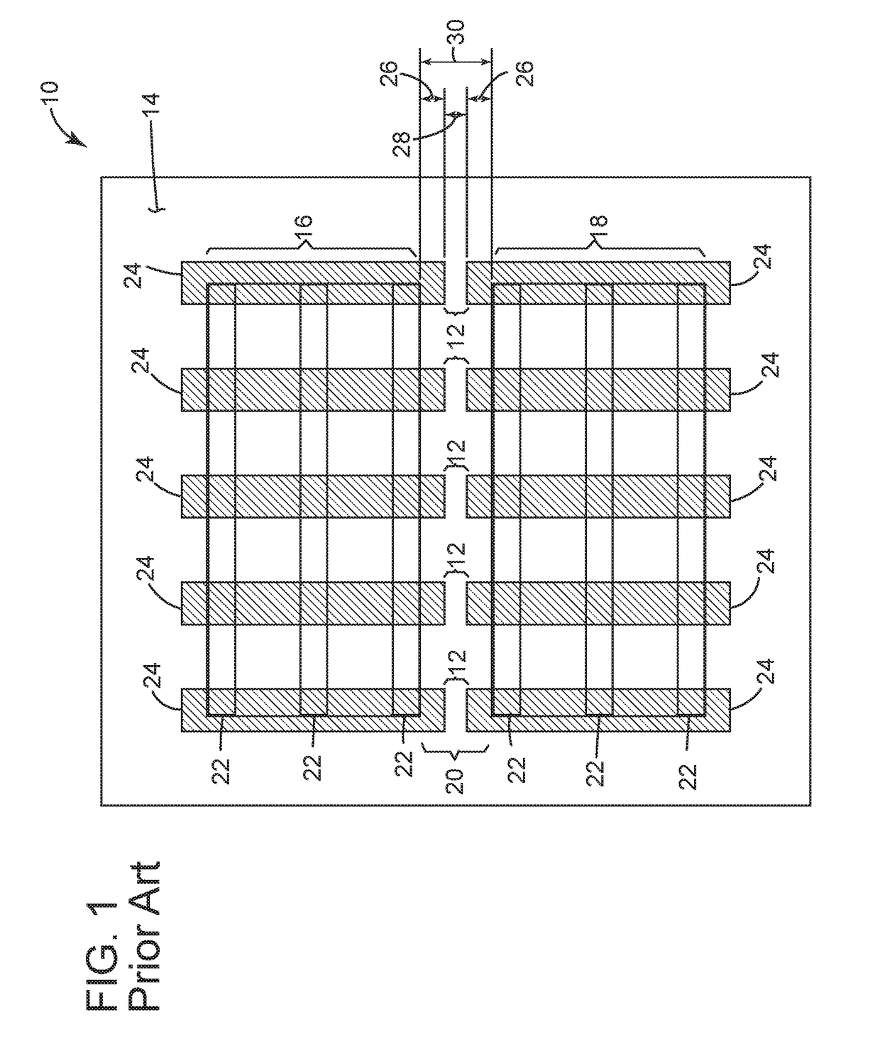
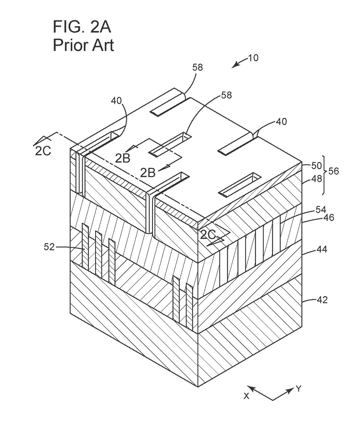
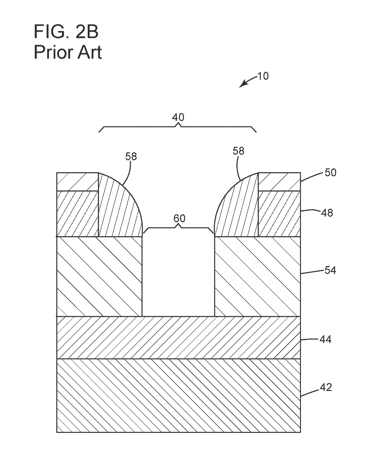
[0028]FIGS. 1-2C illustrate various exemplary embodiments of prior art methods of forming CT pillars. FIGS. 3-9 illustrate various exemplary embodiments of a method of forming CT p...


PUM


Abstract

A method includes providing a semiconductor structure having a substrate and a plurality of fins extending upwards from the substrate. A CT pillar layer is disposed over the semiconductor structure. A CT mask is lithographically patterned over the CT pillar layer. The CT mask is anisotropically etched to remove exposed portions of the CT pillar layer and to form a CT pillar between the fins. A dummy gate structure is disposed across the CT pillar. The dummy gate structure is replaced with first and second metal gate structures that are electrically isolated from each other by the CT pillar.

Description

TECHNICAL FIELD[0001]The present invention relates to semiconductor devices and methods of making the same. More specifically, the invention relates to methods of forming an electrically isolating CT pillar between adjacent gate structures in a semiconductor structure.BACKGROUND[0002]CT pillars terminate the tip ends of gate structures in a semiconductor structure (or semiconductor). CT pillars provide tip to tip electrical isolation between gate structures disposed in separate active (Rx) regions of a semiconductor. In a semiconductor, Rx regions are where a plurality of active devices, such as Fin Field Effect Transistors (FinFETs), are disposed. The Rx regions are separated by isolation regions which have no active devices.[0003]More specifically for FinFETs, these active devices include a source and drain region separated by a channel. The source, drain and channel are embedded in fins which extend longitudinally across an Rx region. The FinFETs also include gate structures whic...

Claims


Application Information

Patent Timeline
Patent Type & Authority Patents(United States)
IPC IPC(8): H01L27/088H01L29/78H01L21/8234H01L29/66H01L21/311H01L21/28H01L27/092H01L25/07H01L27/108
CPCH01L21/823437H01L21/28247H01L21/31111H01L21/823431H01L21/823481H01L29/6653H01L29/66545H01L27/0886H01L29/7831H01L27/0924H01L27/10879H10B12/056
Inventor ZANG, HUIWATTS, JOSEF
Owner GLOBALFOUNDRIES U S INC
Why Eureka
Try Eureka