Method for fabricating junctions and spacers for horizontal gate all around devices

a technology of nanowires and junctions, applied in the field of vertical stacking nanowires, can solve the problems of significant short channel effect, increased processing capacity, and inability to meet the requirements of processing, and achieve the effect of reducing the manufacturing difficulty of integrating all these materials into the nanowire structure without deteriorating the device performan

Active Publication Date: 2019-01-08
APPLIED MATERIALS INC
View PDF7 Cites 15 Cited by
  • Summary
  • Abstract
  • Description
  • Claims
  • Application Information

AI Technical Summary

Problems solved by technology

Reliably producing sub-half micron and smaller features is one of the key technology challenges for next generation very large scale integration (VLSI) and ultra large-scale integration (ULSI) of semiconductor devices.
However, as the limits of circuit technology are pushed, the shrinking dimensions of VLSI and ULSI technology have placed additional demands on processing capabilities.
Furthermore, reduced channel length often causes significant short channel effect with conventional planar MOSFET architecture.
In hGAA structures, different materials are often utilized to form the channel structures (e.g., nanowires), which may undesirably increase the manufa...

Method used


Image

  • Method for fabricating junctions and spacers for horizontal gate all around devices
  • Method for fabricating junctions and spacers for horizontal gate all around devices
  • Method for fabricating junctions and spacers for horizontal gate all around devices

Examples


Embodiment Construction

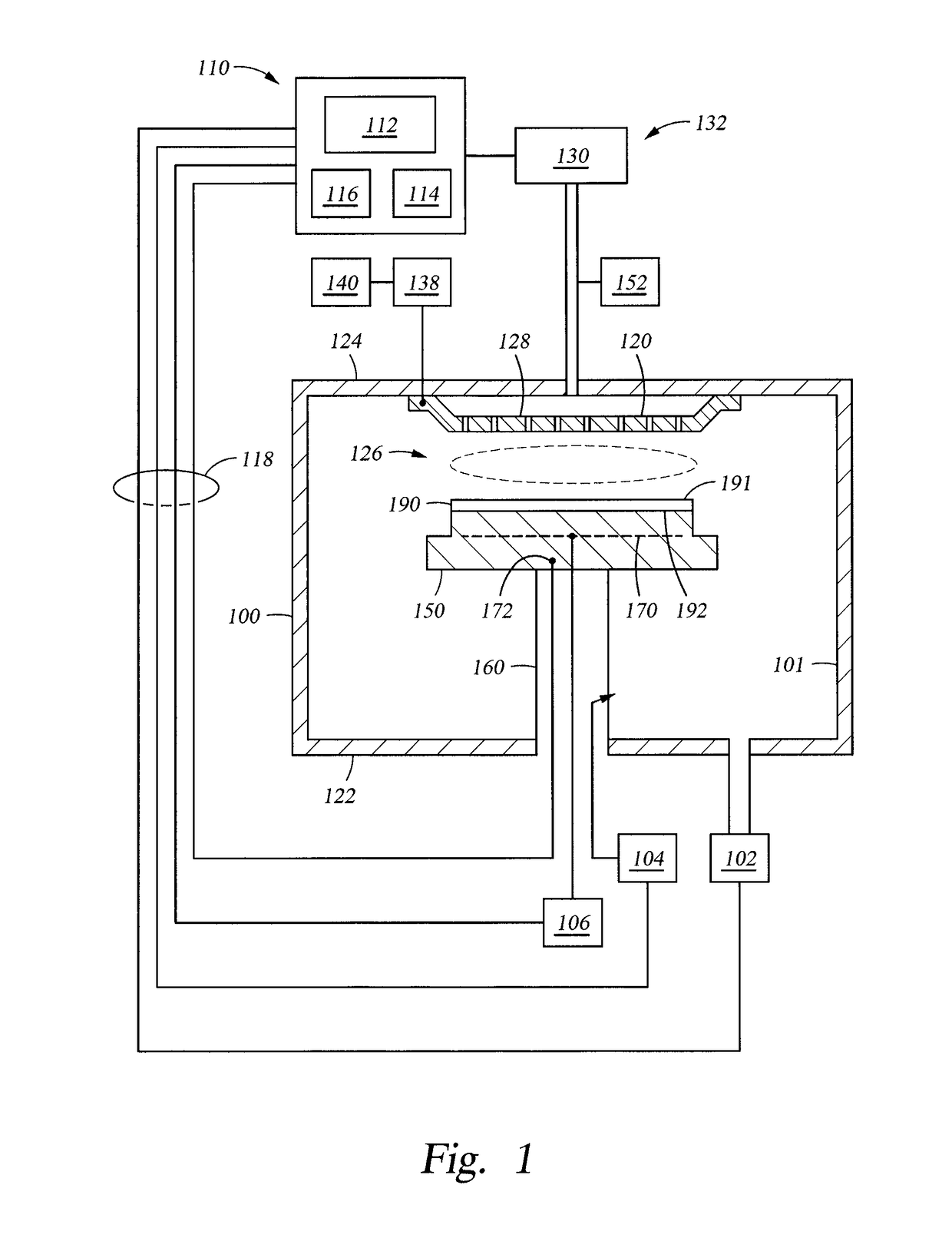
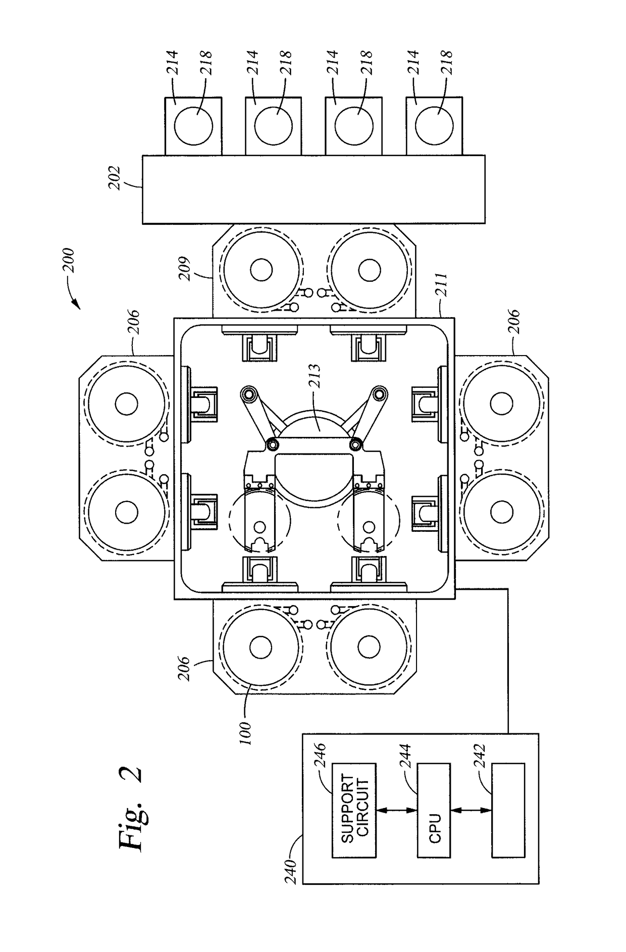
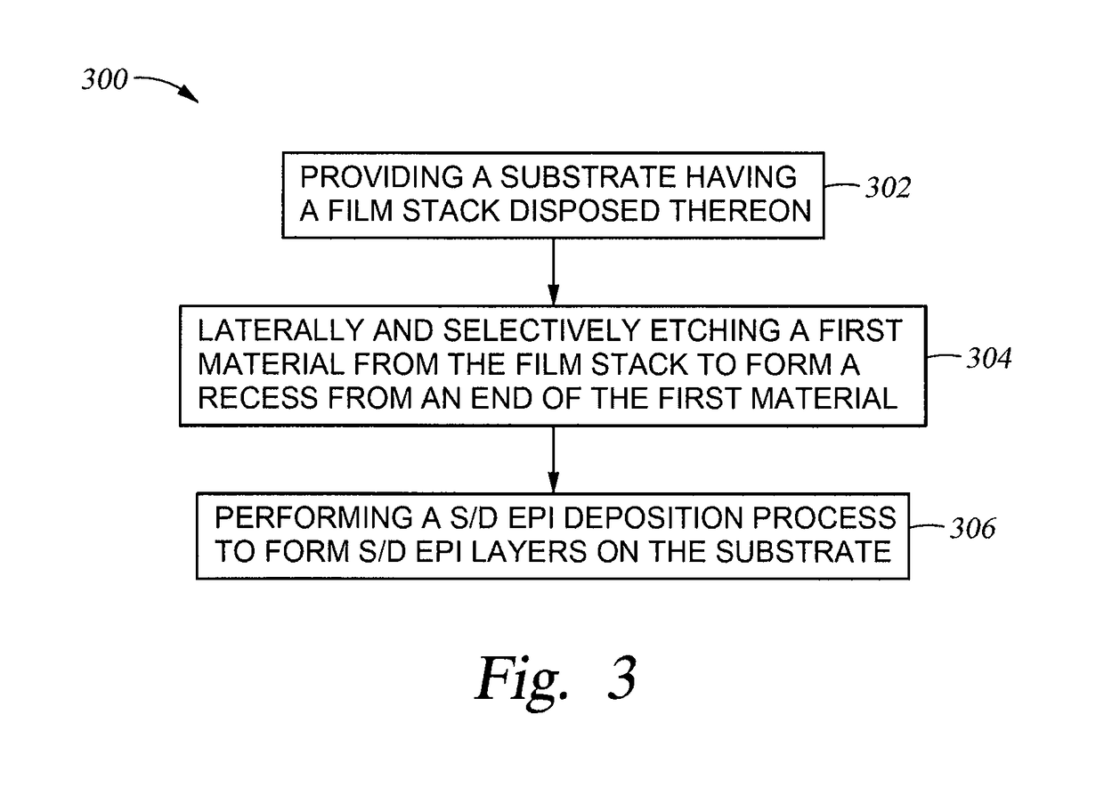
[0021]Methods for manufacturing nanowire structures with controlled parasitic capacitance and resistance for a horizontal gate-all-around (hGAA) semiconductor device structure are provided. In one example, a superlattice structure comprising different materials (e.g., a first material and a second material) arranged in an alternatingly stacked formation may be formed on a substrate to be later utilized as nanowires (e.g., channel structures) for horizontal gate-all-around (hGAA) semiconductor device structures. Several processes may be performed to form source / drain regions adjacent to the nanowire structures with desired single or multiple materials so as to improve electrical performance. Selective etching processes and selective oxidation processes may be performed to selectively etch a pre-determined material at certain locations in the nanowire structures while selectively form another pre-determined material at another locations to form source / drain and their extension reg...


PUM


Abstract

The present disclosure provides methods for forming horizontal gate-all-around (hGAA) structure devices. In one example, a method includes selectively and laterally etching a first group of sidewalls of a first layer in a multi-material layer, wherein the multi-material layer comprises repeating pairs of the first layer and a second layer, the first and the second layers having the first group and a second group of sidewalls respectively, the first group of sidewalls from the first layer exposed through openings defined in the multi-material layer and a group of inner spacers formed atop of the second group of sidewalls from the second layer, forming a recess from the first group of sidewalls of the first layer and defining a vertical wall inward from an outer vertical surface of the inner spacer formed atop of the second layers, and forming an epi-silicon layer from the recess of the first layer.

Description

BACKGROUNDField[0001]Embodiments of the present invention generally relate to methods for forming vertically stacked nanowires with desired materials on a semiconductor substrate, and more particularly to methods for forming vertically stacked nanowires, spacers and junctions on a semiconductor substrate with desired materials for horizontal gate all around devices for semiconductor manufacturing applications.Description of the Related Art[0002]Reliably producing sub-half micron and smaller features is one of the key technology challenges for next generation very large scale integration (VLSI) and ultra large-scale integration (ULSI) of semiconductor devices. However, as the limits of circuit technology are pushed, the shrinking dimensions of VLSI and ULSI technology have placed additional demands on processing capabilities. Reliable formation of gate structures on the substrate is important to VLSI and ULSI success and to the continued effort to increase circuit density and quality...

Claims


Application Information

Patent Timeline
IPC IPC(8): H01L21/02H01L29/423H01L29/417H01L29/786H01L29/66H01L29/06H01L29/78
CPCH01L29/42392H01L29/0673H01L21/02603H01L29/41791H01L29/78696H01L29/785H01L29/66795H01L2029/7858H01L21/3065H01L29/66772H01L29/66439B82Y10/00H01L29/775H01L29/0653H01L29/0847H01L29/66469H01L29/36H01L21/2255H01L21/67742H01L21/67196H01L21/2254H01L29/6656H01L21/76801H01L21/324
Inventor YOSHIDA, NAOMIDONG, LINSUN, SHIYUKIM, MYUNGSUNKIM, NAM SUNGKIOUSSIS, DIMITRIKOROLIK, MIKHAILSANTORO, GAETANOPENA, VANESSA
Owner APPLIED MATERIALS INC
Why Eureka
Try Eureka