
Gate oxide soft breakdown detection circuit

a technology of soft breakdown and detection circuit, which is applied in the field of failures in integrated circuits, can solve the problems of extreme stress on the gate oxide of the transistor during operation, failure of the transistor in time over continuous operation, and the amount of pessimism in the reliability calculation and prediction of the devi

Active Publication Date: 2019-04-02
ADVANCED MICRO DEVICES INC
View PDF3 Cites 0 Cited by
  • Summary
  • Abstract
  • Description
  • Claims
  • Application Information

AI Technical Summary

Problems solved by technology

In general, the gate oxide of a transistor is subjected to extreme stress during operation, e.g., stresses due to high overshoots and undershoots of a signal applied to the gate of the transistor or stresses due to power supply over-voltages used to boost the performance of the transistor and associated system.
Those higher electric fields stress gate oxide structures and cause failures of the transistors in time over continuous operation.
This assumption causes an amount of pessimism in the device reliability calculations and predictions based on that methodology.

Method used


Image

  • Gate oxide soft breakdown detection circuit
  • Gate oxide soft breakdown detection circuit
  • Gate oxide soft breakdown detection circuit

Examples


Embodiment Construction

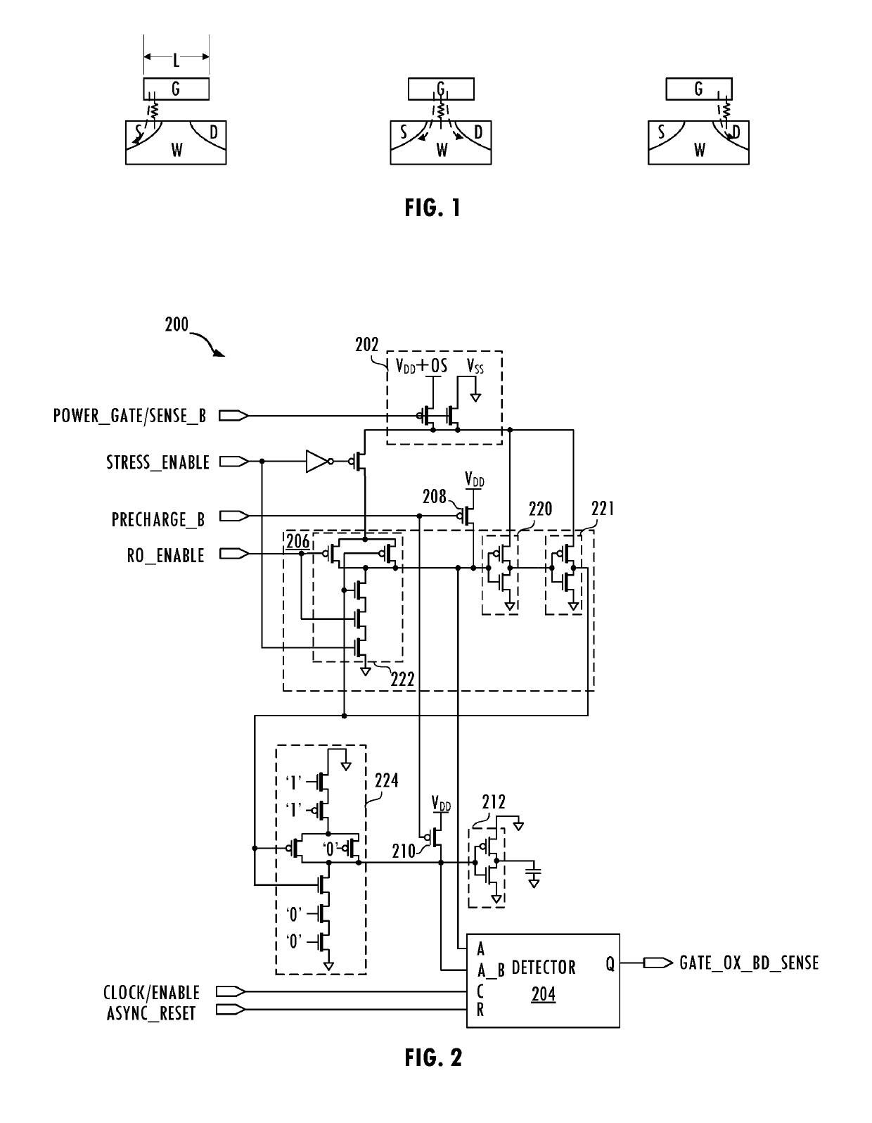
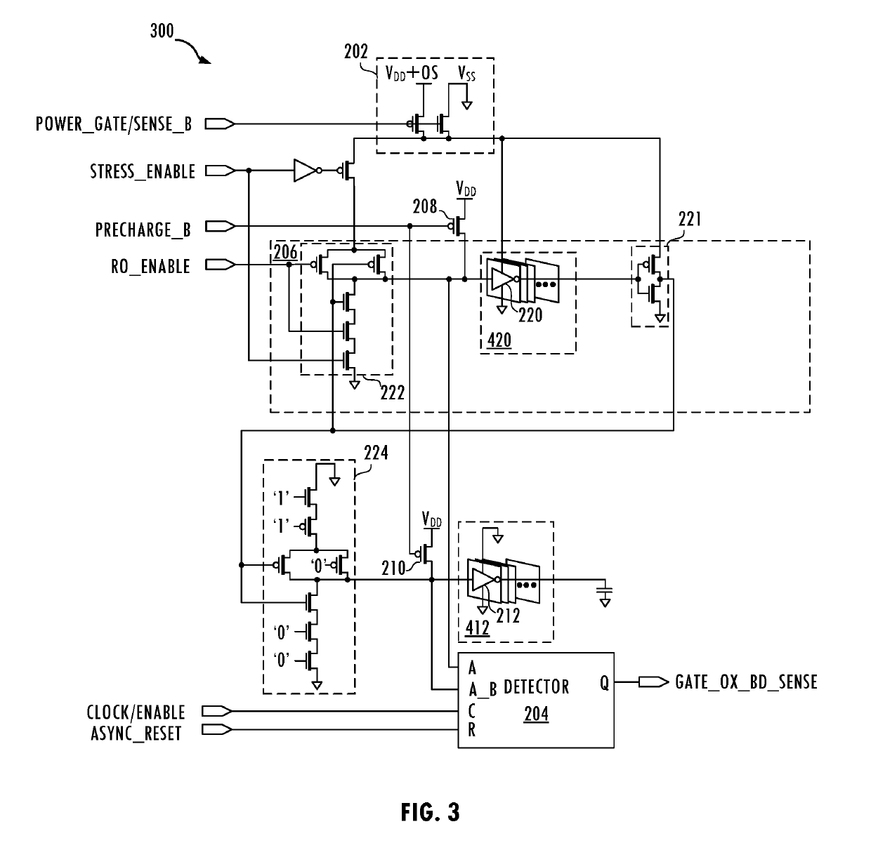
[0005]In at least one embodiment, an apparatus for detecting a breakdown of gate oxide of a transistor includes a first instance of a device responsive to a first node. The first instance of the device is configured to be stressed in a first mode of the apparatus and to be unstressed in a second mode of the apparatus. The apparatus includes a second instance of the device responsive to a second node, a power control circuit configured to couple a first high voltage reference input of the first instance of the device to a first power supply node in the first mode of the apparatus and to couple the first high voltage reference input of the first instance of the device to a second power supply node in the second mode of the apparatus. The apparatus includes a precharge circuit configured to selectively precharge the first node and the second node in response to a precharge control signal in the second mode of the apparatus. The apparatus includes a voltage difference detection circuit ...


PUM


Abstract

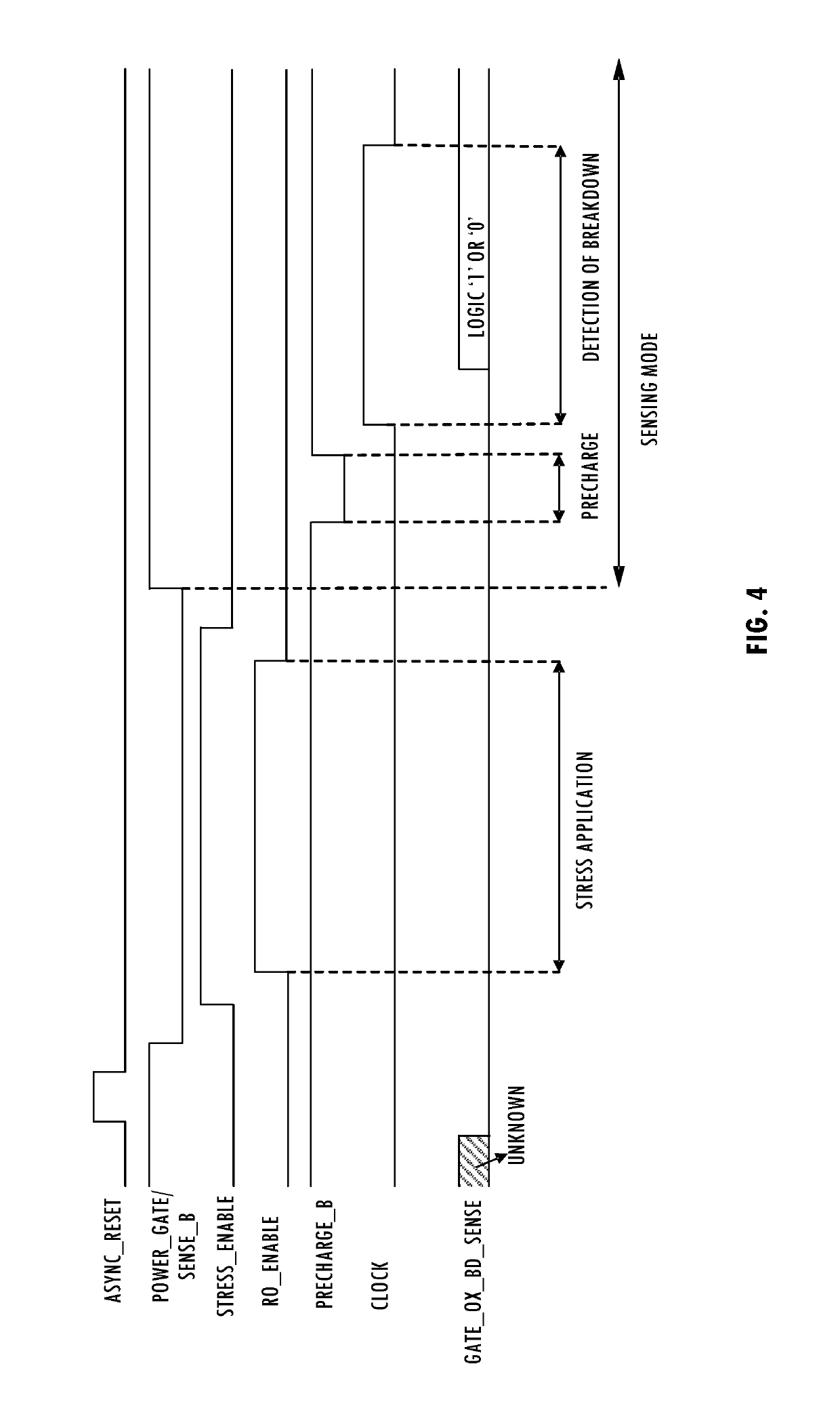
Various embodiments of a gate oxide breakdown detection technique detect gate oxide degradation due to stress on a per part basis without destroying functional circuits for an intended application. Stress on the gate oxide may be applied while nominal drain currents flow through a device, thereby stressing the device under conditions similar to actual operating conditions. The technique is relatively fast and does not require analog amplifiers or tuning of substantial amounts of other additional circuitry as compared to conventional gate oxide breakdown detection techniques.

Description

BACKGROUND[0001]Field of the Invention[0002]The present invention is related to integrated circuits and more particularly to failures in integrated circuits.[0003]Description of the Related Art[0004]In general, the gate oxide of a transistor is subjected to extreme stress during operation, e.g., stresses due to high overshoots and undershoots of a signal applied to the gate of the transistor or stresses due to power supply over-voltages used to boost the performance of the transistor and associated system. As semiconductor manufacturing technology shrinks transistor dimensions, the gate oxide thickness also decreases, causing higher electric fields to be observed by the gate oxide. Those higher electric fields stress gate oxide structures and cause failures of the transistors in time over continuous operation. Therefore, it is desirable to evaluate the failure rates of transistors due to gate oxide degradation in response to high dielectric stresses. Time Dependent Dielectric Breakd...

Claims


Application Information

Patent Timeline
Patent Type & Authority Patents(United States)
IPC IPC(8): G01R31/26H03K5/159H03K3/03
CPCG01R31/2623H03K5/159H03K3/0315
Inventor DESHPANDE, ABHAYIYER, ARUN S.VALLUR, PRASANTH K.SINGRIGOWDA, GIRISH ANATHAHALLYKOSONOCKY, STEPHEN V.
Owner ADVANCED MICRO DEVICES INC
Learn More