FFS type TFT array substrate and the manufacturing method thereof

a technology of array substrates and ffs, applied in the field of display technology, can solve the problems of relatively high current fabrication cost of ffs type tft array substrates, and achieve the effect of low production cost and less photomask processes

Inactive Publication Date: 2019-05-28
SHENZHEN CHINA STAR OPTOELECTRONICS SEMICON DISPLAY TECH CO LTD
View PDF10 Cites 0 Cited by
  • Summary
  • Abstract
  • Description
  • Claims
  • Application Information

AI Technical Summary

Benefits of technology

[0005]An object of the present invention is to provide a method for fabricating an FFS type TFT array substrate, which uses less photomask processes and low production cost.
[0006]An object of the present invention is to further provide an FFS type TFT array substrate with a simple fabrication process, low production cost and excellent electrical performance.
[0044]The beneficial effects of the present invention are: The manufacturing method for an FFS type TFT array substrate of the present invention comprises that a gate electrode, a scanning line, a common electrode, and a common electrode line are formed in one photomask process. Comparing with the conventional art, the present invention simplifies the manufacturing process, with fewer photomasks, and a shorter processing time, therefore, the production cost is low. The fabrication process of the FFS type TFT array substrate of the invention is simple, has low production cost and excellent electrical performance.

Problems solved by technology

Due to the high fabrication cost of the photomask and the long process time of the 6 photomask processes, the current fabrication cost of the FFS type TFT array substrate is relatively high.

Method used


Image

  • FFS type TFT array substrate and the manufacturing method thereof
  • FFS type TFT array substrate and the manufacturing method thereof
  • FFS type TFT array substrate and the manufacturing method thereof

Examples


Embodiment Construction

[0061]To further illustrate the technical solutions adopted by the present invention and the effects thereof, the following describes the preferred embodiments of the present invention and the accompanying drawings in detail.

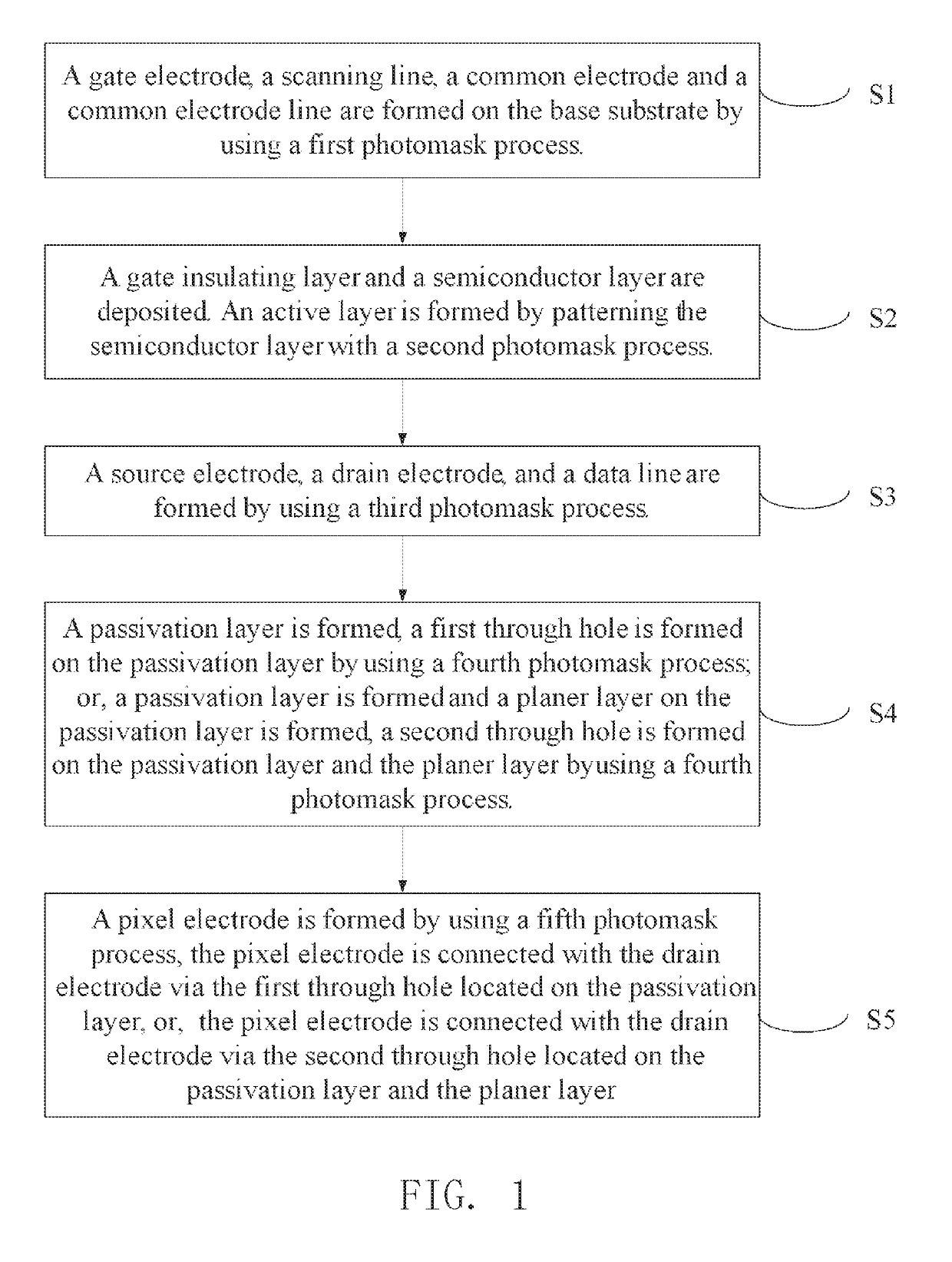
[0062]Please refer to FIG. 1, the present invention provides a manufacturing method for an FFS type TFT array substrate, which comprises below steps:

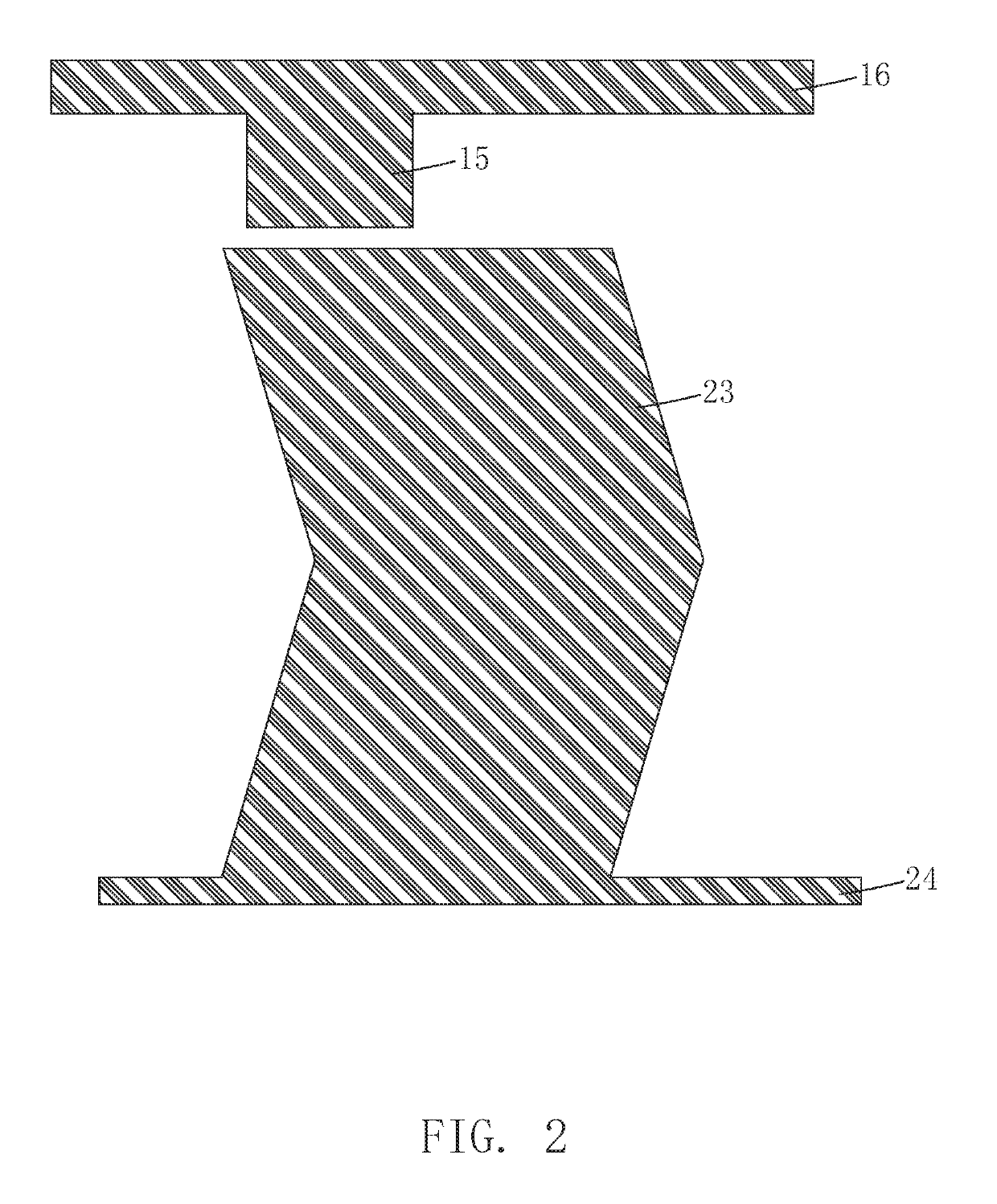
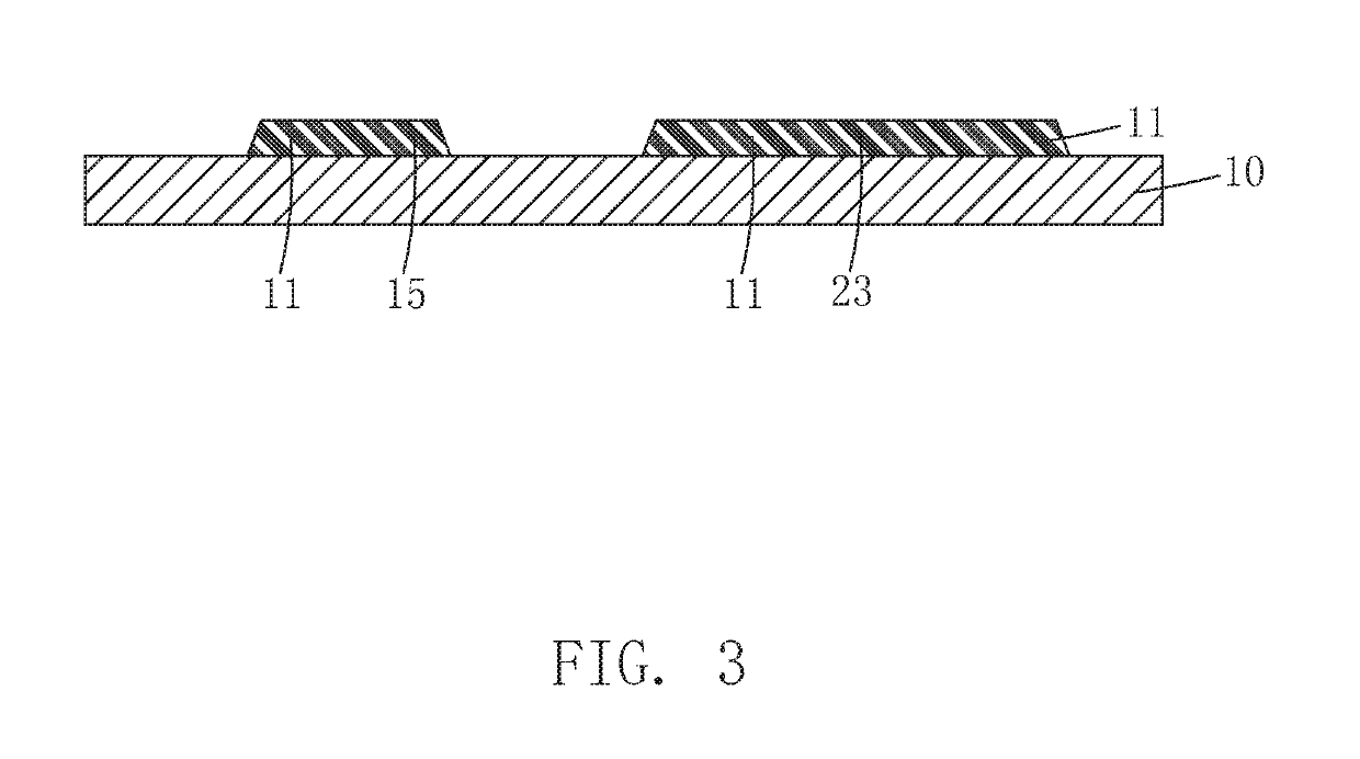
[0063]S1, as shown in FIGS. 2-5. A base substrate 10 is provided. A gate electrode 21, a scanning line 22, a common electrode 23 and a common electrode line 24 are formed on the base substrate 10 by using a first photomask process. The gate electrode 21 is connected with the scanning line 22. The common electrode 23 is connected with the common electrode line 24.

[0064]Specifically, the step of forming a gate electrode 21, a scanning line 22, a common electrode 23 and a common electrode line 24 on the base substrate 10 by using a first photomask process further comprises:

[0065]S11, as shown in FIGS. 2-3. A first tran...


PUM

PropertyMeasurementUnit
transparent conductiveaaaaaaaaaa
transparentaaaaaaaaaa
conductivityaaaaaaaaaa

Abstract

The present invention provides an FFS type TFT array substrate and a manufacturing method thereof. The manufacturing method for an FFS type TFT array substrate of the present invention comprises that a gate electrode, a scanning line, a common electrode, and a common electrode line are formed in one photomask process. Comparing with the conventional art, the present invention simplifies the manufacturing process, with fewer photomasks, and a shorter processing time, therefore, the production cost is low. The fabrication process of the FFS type TFT array substrate of the present invention is simple, has low production cost and excellent electrical performance.

Description

BACKGROUND OF THE INVENTIONField of Invention[0001]The present invention relates to the field of display technology, and more particularly to a fringe field switching (FFS) thin film transistor (TFT) array substrate and a manufacturing thereof.Description of Prior Art[0002]Liquid crystal displays (LCDs) such as flat panel display devices are widely used in mobile phones, televisions, personal digital assistants, digital cameras, notebooks, desktop, other consumer electronics products and etc. for high quality, power saving, thin body and wide application range. The LCDs has become the mainstream in display device.[0003]Most of the liquid crystal display (LCD) devices on the market are backlight type LCDs, which comprise a LCD panel and a backlight module. In general, the LCD panel is composed of a color filter (CF) substrate, a thin film transistor (TFT) substrate, a liquid crystal (LC) sandwiched between the CF substrate and the TFT substrate, and a sealant frame sealant.[0004]TFT-...

Claims


Application Information

Patent Timeline
Patent Type & Authority Patents(United States)
IPC IPC(8): H01L27/12G02F1/1343
CPCH01L27/124G02F1/134309H01L27/127H01L27/1288H01L27/1237G02F2201/123G02F2001/134372G02F2201/121H01L29/41733H01L27/1248H01L27/1259G02F1/134363G02F1/134372G02F1/136231
Inventor ZHOU, ZHICHAOXIA, HUICHEN, MENG
Owner SHENZHEN CHINA STAR OPTOELECTRONICS SEMICON DISPLAY TECH CO LTD
Why Eureka
Try Eureka