

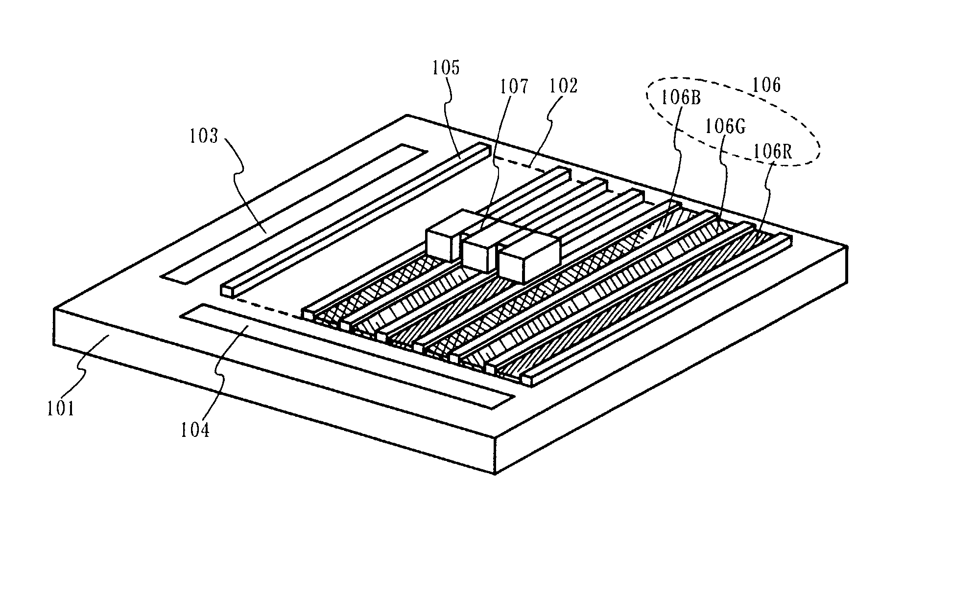
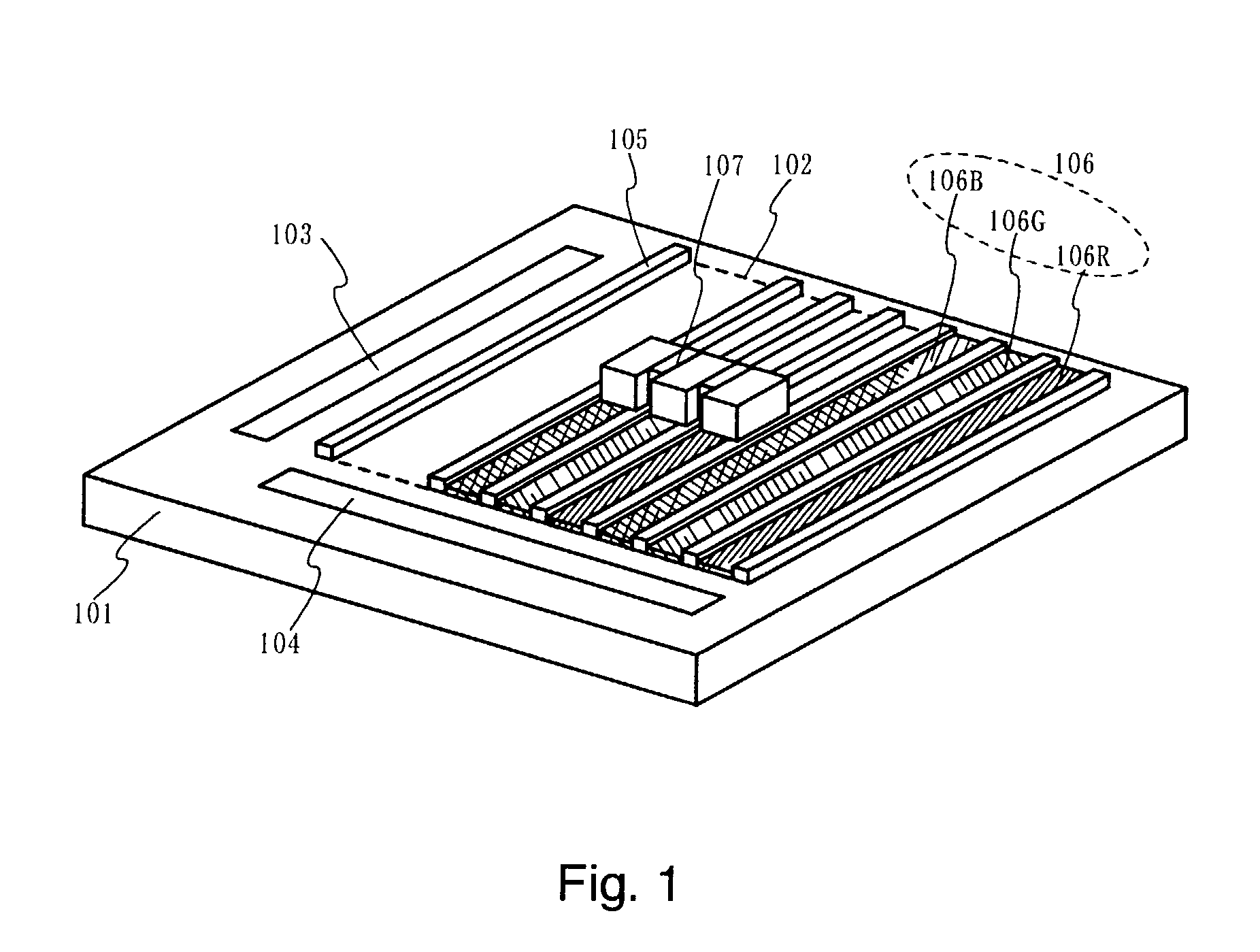
Method of manufacturing a light emitting device
- Summary
- Abstract
- Description
- Claims
- Application Information
AI Technical Summary
Benefits of technology
Problems solved by technology
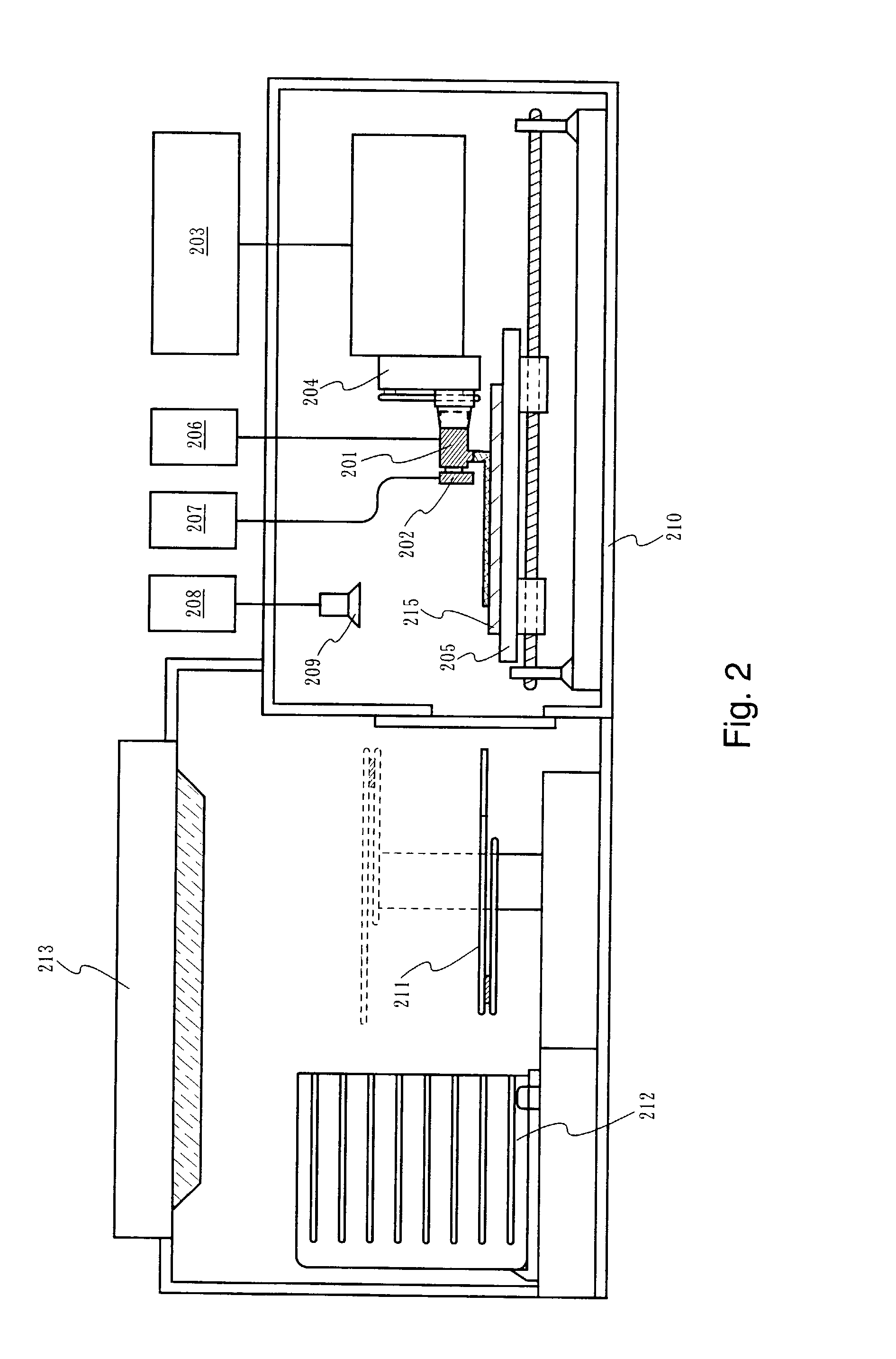
Method used
Image

Examples
embodiment 1
[0077] Embodiment 1
[0078] As shown in FIG. 12A, transparent pixel electrodes 1201 to 1204 are formed on a substrate 1200 at a pitch of 40 to 120 .mu.m and having a thickness of 0.1 .mu.m. Indium oxide, zinc oxide, tin oxide, or a mixed compound of these oxides is used as a material for forming the transparent pixel electrodes.
[0079] Next, as sown in FIG. 12B, partitions 1205 made from a resin material are formed between the pattern of the transparent pixel electrodes. The partitions have a thickness of 1 to 2 .mu.m, a width of 20 .mu.m, and are formed so as to cover edge portions of the transparent pixel electrodes. The partitions are formed so that compositions discharged from an ink head and impacting on the transparent pixel electrodes do not flow out and mix into the adjacent pixels.
[0080] Next, a first organic compound layer is formed having a thickness of 30 nm on the glass substrate 1200 having the transparent pixel electrodes (anodes) 1201 to 1204 by a spinning application m...
embodiment 2
[0083] Embodiment 2
[0084] FIGS. 13A to 13D show an example of manufacturing an active matrix drive light emitting device by an ink jet method using the manufacturing method of the present invention. In FIG. 13A, thin film transistors 1301 to 1303 as active elements are formed on a substrate 1300. The thin film transistors are composed of a semiconductor film in which portions such as channel forming regions, source regions, and drain regions are formed, gate electrodes, gate insulating films, and the like. The structure of the thin film transistors has characteristics that differ depending upon type, such as top gate and bottom gate types, but there are no limitations placed on the type of structure when applying the present invention.
[0085] Pixel electrodes 1304 to 1306 connected to source or drain regions of the thin film transistors are formed at a pitch of 65 .mu.m and having a thickness of 0.1 .mu.m, for example. A minute pattern can be formed without the pattern being drawn ou...
embodiment 3
[0090] Embodiment 3
[0091] A specific example of a light emitting device manufactured by an ink jet method using a composition of the present invention is explained with reference to the figures. FIG. 14 shows a top view of an example of a pixel structure for an active matrix light emitting device. Further, FIG. 15 is a cross sectional view corresponding to FIG. 14 cut along a line segment A-A'. The pixel structure is explained with both figures using common reference numerals.
[0092] The pixel structure has two thin film transistors formed in one pixel. One thin film transistor is an n-channel thin film transistor 1604 used for switching operation, and the other is a p-channel thin film transistor 1605 used for controlling electric current flowing in an organic light emitting element. Of course, there is no need to limit the number of thin film transistors formed per one pixel when manufacturing an active matrix drive light emitting device using an ink jet printing apparatus of the p...
PUM
 Abstract
Description
Claims
Application Information