Compound solar cell and production method therefor

a solar cell and production method technology, applied in the field of compound solar cells, can solve problems such as productivity reduction, and achieve the effects of preventing the reduction of conversion efficiency, and reducing the cost of production

Inactive Publication Date: 2019-05-28
NITTO DENKO CORP
View PDF26 Cites 0 Cited by
  • Summary
  • Abstract
  • Description
  • Claims
  • Application Information

AI Technical Summary

Benefits of technology

[0008]In view of the foregoing, it is an object of the present invention to provide a compound solar cell which can be produced by sequentially performing the process steps without the need for performing the buffer layer forming step in the atmospheric environment and yet has a higher conversion efficiency, and a production method for the compound solar cell.
[0011]In the inventive compound solar cell, the interface layer made of the mixed crystal compound having the composition represented by the above general formula (1) is provided between the compound light absorbing layer and the buffer layer. The compound light absorbing layer is in contact with the interface layer made of the mixed crystal compound which has a crystal orientation generally perpendicular to a surface of the compound light absorbing layer. Therefore, lattice defects are less liable to occur in the interface between the compound light absorbing layer and the interface layer, so that the recombination of the carriers is effectively suppressed. This prevents the reduction in conversion efficiency. Further, the buffer layer is provided on the interface layer having a crystal orientation perpendicular to the surface of the compound light absorbing layer. Influenced by the crystal orientation of the interface layer, therefore, the buffer layer easily has a crystal orientation perpendicular to the surface of the compound light absorbing layer. Therefore, electrons generated in the light absorbing layer easily reach the front side electrode layer, so that the recombination is suppressed. In the inventive compound solar cell, the compound light absorbing layer is made of the Group I-III-VI compound semiconductor and, therefore, has a higher conversion efficiency even in the form of a thin film. Since the reduction in conversion efficiency is prevented, the inventive compound solar cell has excellent characteristic properties.
[0014]Where the steps of forming the compound light absorbing layer of the Group I-III-VI compound semiconductor over the elongated substrate while transporting the substrate in the longitudinal direction, forming the interface layer, forming the buffer layer, and forming the front side electrode layer are performed sequentially in this order in a vacuum in the method for producing the compound solar cell according to the first aspect, there is no need to once take out the substrate over which the compound light absorbing layer is formed into the atmospheric environment to perform the buffer layer forming step after performing the compound light absorbing layer forming step in a vacuum, and then perform the front side electrode layer forming step again in the vacuum. Therefore, the compound solar cell can be efficiently produced at lower costs as having excellent characteristic properties.

Problems solved by technology

Therefore, these steps cannot be sequentially performed, resulting in reduction in productivity.

Method used


Image

  • Compound solar cell and production method therefor
  • Compound solar cell and production method therefor
  • Compound solar cell and production method therefor

Examples


example 1

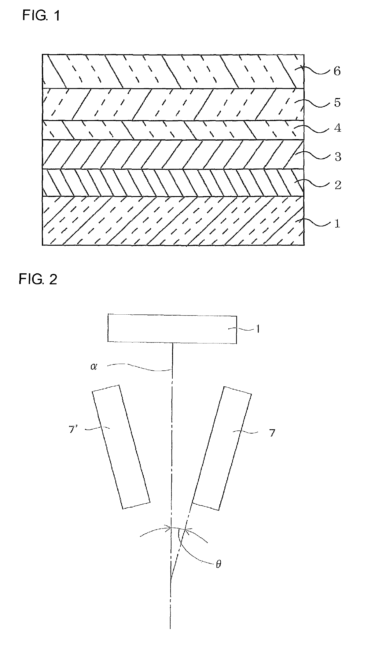
[0051](Formation of Back Side Electrode Layer)

[0052]On a degreased surface of a soda-lime glass substrate (having a thickness of 0.55 mm, a width of 20 mm and a length of 20 mm, and having a square shape as seen in plan), a back side electrode layer of Mo having a thickness of 0.8 μm was formed at a sputtering rate of 60 nm / min at a sputtering pressure of 1 Pa in an argon discharge gas with the use of a direct current (DC) power source by means of a magnetron sputtering apparatus (SH-450 available from Ulvac Inc.)

[0053](Formation of CIGS Light Absorbing Layer)

[0054]Next, a CIGS light absorbing layer was formed on the back side electrode layer formed in the aforementioned manner. That is, Ga, In, Cu, Se evaporation sources were placed in a chamber of the vacuum vapor deposition apparatus, and In, Ga and Se were simultaneously evaporated for 32 minutes with the chamber kept at a vacuum degree of 1×10⁻⁴ Pa and with the substrate temperature kept at 250° C. Thereafter, Cu and Se were si...

examples 2 to 27

[0061]CIGS solar cells were produced in substantially the same manner as in Example 1, except that conditions for the production were changed as shown below in Tables 1 to 3.


PUM


Abstract

A compound solar cell having a higher conversion efficiency and a method for producing the compound solar cell at lower costs are provided. The compound solar cell includes a CIGS light absorbing layer, a buffer layer and a front side electrode layer provided on a substrate. An interface layer made of a mixed crystal compound having a composition represented by the following general formula is provided between the CIGS light absorbing layer and the buffer layer: Zn(Ox,S1-x) . . . (1), wherein X is 0.9<X≤1.

Description

TECHNICAL FIELD[0001]The present invention relates to a compound solar cell which includes a light absorbing layer formed of a Group I-III-VI compound semiconductor such as a CuInSe2 (CIS) compound semiconductor composed of Group I, III and VI elements or a Cu(In,Ga)Se2 (CIGS) compound semiconductor prepared in the form of solid solution by incorporating Ga into CuInSe2, and has a higher photoelectric conversion efficiency (hereinafter referred to as “conversion efficiency”), and a method for efficiently producing the compound solar cell.BACKGROUND ART[0002]Out of various types of solar cells, compound solar cells including a light absorbing layer formed of a CIS or CIGS (hereinafter referred to as “CIGS type”) compound semiconductor are known to be advantageous in that they can be produced in the form of a thin film as having a higher conversion efficiency and are less liable to suffer from reduction in conversion efficiency due to light irradiation or the like.[0003]Conventionally...

Claims


Application Information

Patent Timeline
Patent Type & Authority Patents(United States)
IPC IPC(8): H01L31/032H01L31/18H01L31/0749
CPCH01L31/0322H01L31/0749H01L31/18Y02P70/521Y02E10/541Y02P70/50
Inventor TERAJI, SEIKIKAWAMURA, KAZUNORINISHII, HIROTOWATANABE, TAICHIYAMAMOTO, YUSUKE
Owner NITTO DENKO CORP
Why Eureka
Try Eureka