Range sensor and solid-state imaging device

a solid-state imaging and sensor technology, applied in the field of range sensor and solid-state imaging devices, can solve the problems of large power consumption, large load capacitance of a plurality, dark current, etc., and achieve the effects of high sensitivity, high sensitivity, and high-speed modulation

Active Publication Date: 2019-06-18
NAT UNIV CORP SHIZUOKA UNIV
View PDF21 Cites 7 Cited by
  • Summary
  • Abstract
  • Description
  • Claims
  • Application Information

AI Technical Summary

Benefits of technology

[0012]According to the present invention, it is possible to achieve a range sensor having a large light receiving area and capable of high-speed modulation with high sensitivity at a low dark current, and a solid-state imaging device including a plurality of range sensors as pixels arranged on a semiconductor chip.

Problems solved by technology

In the image sensor disclosed in PTL 1, load capacitances of a plurality of transfer gates connected in parallel increase, and the entire power consumption increases as the number of pixels increases.
Further, connecting a plurality of lock-in pixel elements increases the area of a diffusion layer of a signal detector, which may cause a dark current.

Method used


Image

  • Range sensor and solid-state imaging device
  • Range sensor and solid-state imaging device
  • Range sensor and solid-state imaging device

Examples


first embodiment

[0076](First Embodiment)

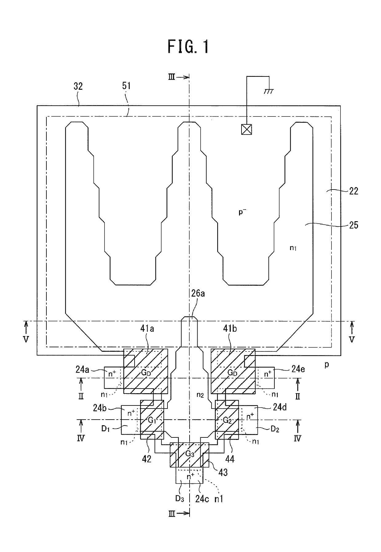
[0077]A range sensor according to the first embodiment of the present invention is a lock-in pixel including a shielding plate 51 having an aperture indicated by the dashed-dotted line in FIG. 1 defining a light-receiving area. As shown in the schematic plan view from above of the principal part of the range sensor in FIG. 1, the range sensor according to the first embodiment is provided with the shielding plate 51 including the aperture opened in a region corresponding to a photodiode of the light-receiving area, and further provided with a pixel region, excluding the aperture, covered with the shielding plate 51 so as to be shielded from light.

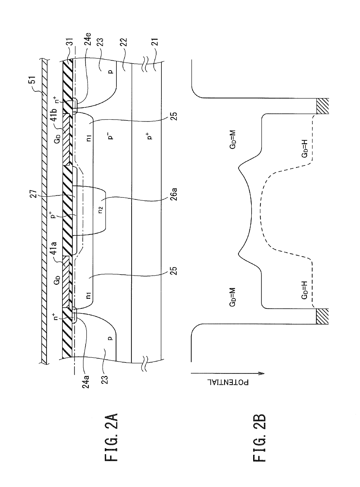
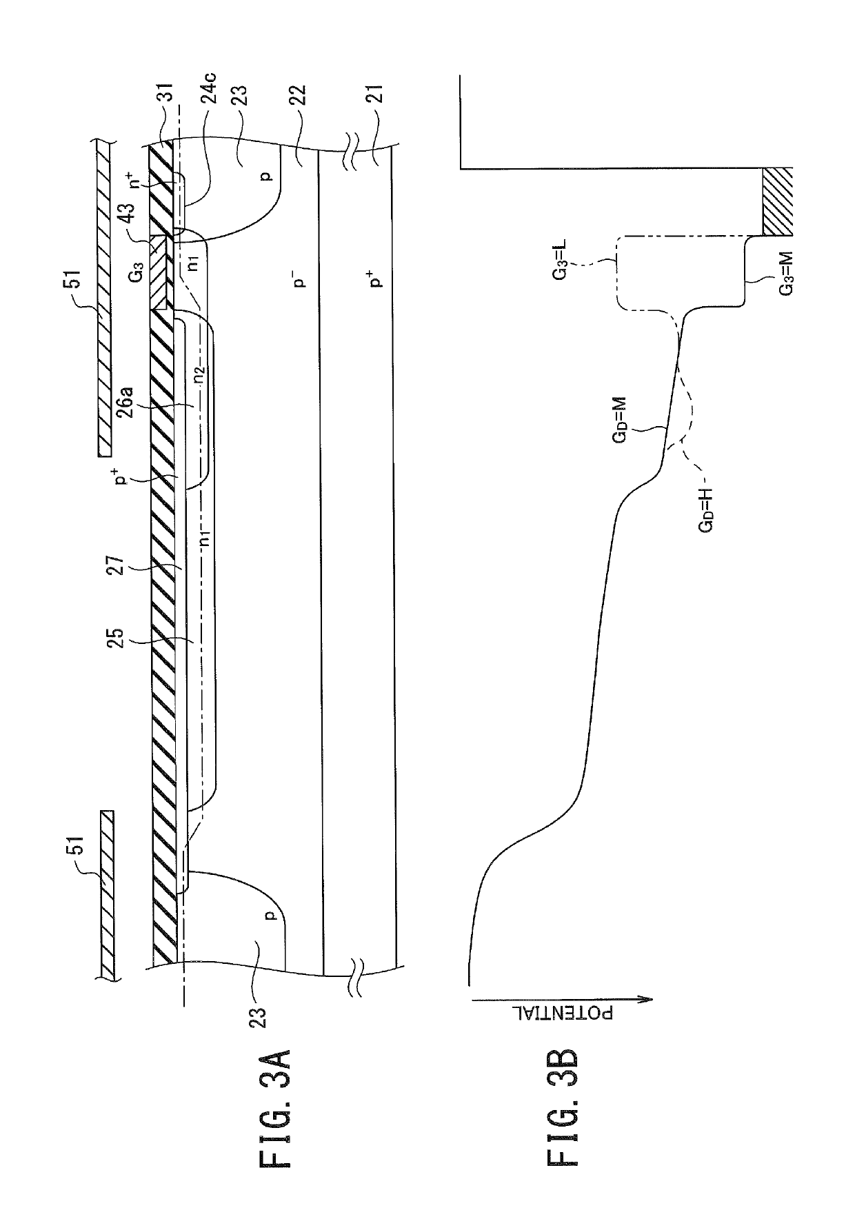
[0078]The range sensor according to the first embodiment serves as a lock-in pixel. As understood from the cross-sectional views of FIG. 2 to FIG. 4, the lock-in pixel includes a pixel layer 22 made of a semiconductor of a first conductivity type (p-type), the shielding plate 51 having the aperture and provided above ...

second embodiment

[0124](Second Embodiment)

[0125]A range sensor according to the second embodiment of the present invention is a lock-in pixel including a shielding plate 51 having an aperture indicated by the dashed-dotted line in FIG. 15 to define a light-receiving area. The range sensor according to the second embodiment fundamentally has the same structure as the range sensor according to the first embodiment, as shown in the cross-sectional views of FIG. 2 to FIG. 4, and serves as a lock-in pixel including: a pixel layer 22 made of a semiconductor of a first conductivity type (p-type); the shielding plate 51 having the aperture and provided above the pixel layer 22 to define the light-receiving area on the pixel layer 22 below the aperture; a surface-buried region 25 of a second conductivity type (n-type) selectively buried in the upper portion of the pixel layer 22 to implement a photodiode in the light-receiving area by forming a junction with the pixel layer 22, and extending from the light-r...

third embodiment

[0137](Third Embodiment)

[0138]A range sensor according to the third embodiment of the present invention is a lock-in pixel including a first surface-buried region 25u and a second surface-buried region 25v opposed in an interdigital manner inside a light-receiving area defined by a shielding plate 51 having a single aperture indicated by the dashed-dotted line as shown in the schematic plan view from above of the principal part in FIG. 16. Reference numeral 32b shown in FIG. 16 denotes an edge of a field insulating film. Namely, an area surrounded by the edge 32b defines an active area of the lock-in pixel. The range sensor according to the third embodiment thus includes two surface-buried regions in one pixel. As in the case shown in the cross sections of FIG. 2A, FIG. 3A and FIG. 4A, a p-type well region 23 is buried below the field insulating film (not shown).

[0139]When focused on the first surface-buried region 25u provided in the light-receiving area on the upper side in FIG. 1...


PUM


Abstract

A range sensor includes: an n-type surface-buried region selectively buried in an upper portion of a pixel layer to implement a photodiode and extending from a light-receiving area toward plural portions shielded by a shielding plate along the upper portion of the pixel layer so as to provide a plurality of branches; n-type charge-accumulation regions having a higher impurity concentration than the surface-buried region; a plurality of transfer gate electrodes provided adjacent to the charge-accumulation regions; and an n-type guide region having a higher impurity concentration than the surface-buried region and a lower impurity concentration than the charge-accumulation regions, and provided with one end below an aperture of the shielding plate and other ends extending to a part of the respective transfer gate electrodes.

Description

TECHNICAL FIELD[0001]The present invention relates to a range sensor having a lock-in pixel function for detecting photoelectrons in synchronization with a light pulse, and a solid-state imaging device including a plurality of range sensors arranged as pixels.BACKGROUND ART[0002]In recent years, development of time-of-flight range image sensors using semiconductors is actively being carried out. For example, a range image sensor includes a plurality of lock-in pixels arrayed and connected in parallel for transferring carriers generated in photodiodes in synchronization with a light source to a plurality of charge accumulators, while each lock-in pixel element is made into a smaller pixel so as to transfer charges at high speed as disclosed in Patent Literature (PTL) 1.[0003]In the image sensor disclosed in PTL 1, load capacitances of a plurality of transfer gates connected in parallel increase, and the entire power consumption increases as the number of pixels increases. Further, co...

Claims


Application Information

Patent Timeline
Patent Type & Authority Patents(United States)
IPC IPC(8): G01S7/481H04N5/3745H01L27/144H01L27/146H01L31/10H04N5/369H04N5/374H04N5/361
CPCH01L27/14638G01S7/481H01L27/144H01L27/146H01L27/14605H01L27/14623H01L27/14643H01L31/10H04N5/361H04N5/369H04N5/374H04N5/3745H01L27/14603H04N25/63H04N25/70H04N25/77H04N25/76H01L27/14683
Inventor KAWAHITO, SHOJI
Owner NAT UNIV CORP SHIZUOKA UNIV
Why Eureka
Try Eureka