Array substrate and liquid crystal display panel

a liquid crystal display and array substrate technology, applied in non-linear optics, instruments, optics, etc., can solve the problems affecting the display effect and the yield of products, and achieve the effect of effectively shielding external static electricity and improving the antistatic ability of the array substra

Active Publication Date: 2019-07-09
WUHAN CHINA STAR OPTOELECTRONICS TECH CO LTD
View PDF8 Cites 0 Cited by
  • Summary
  • Abstract
  • Description
  • Claims
  • Application Information

AI Technical Summary

Benefits of technology

[0005]In view of this, the present disclosure provides an array substrate and a liquid crystal display panel having an electrostatic protection structure for effectively shielding external static electricity and improving the antistatic ability of the array substrate and the panel.
[0007]Preferably, the electrostatic protection structure is enclosed around the periphery of the array substrate, the periphery of each array block, and the periphery of the display area of each sub-array substrate. In this way, static electricity can be well prevented from entering the signal lines and the display area during transportation, cutting and thinning of the substrate and the panel including the substrate, so that better electrostatic protection can be achieved on the substrate.
[0011]In this case, using the annular transparent conductive metal oxide wire as an electrostatic protection structure can surround at least one of the periphery of the array substrate, the periphery of each array block, and the periphery of the display region of each sub-array substrate. The transparent conductive metal material has high conductivity and good conductivity. In this way, the substrate and the panel including the substrate can be well shielded from static electricity during transportation, cutting and thinning to prevent the static electricity from entering the signal lines and the display area, thereby achieving better electrostatic protection.
[0014]In this case, the transparent conductive layer and the metal layer are electrically connected in the up-down direction through the via holes in the protective layer to jointly form the electrostatic protection structure, the electrostatic protection structure is equivalent to the transparent conductive layer and the metal layer connected in parallel, which is better than the conductivity when the annular transparent conductive layer is used alone, and has the better anti-static impact effect. Moreover, at least one of the periphery of each array block and the periphery of the display area of each sub-array substrate is arranged around the periphery of the array substrate, so that the substrate can be better protected from electrostatic damage.

Problems solved by technology

Static electricity can be easily introduced into the liquid crystal panel to cause electrostatic damage to the internal components of the panel, thereby affecting the display effect and greatly affecting the yield of the product.

Method used


Image

  • Array substrate and liquid crystal display panel
  • Array substrate and liquid crystal display panel
  • Array substrate and liquid crystal display panel

Examples


embodiment 1

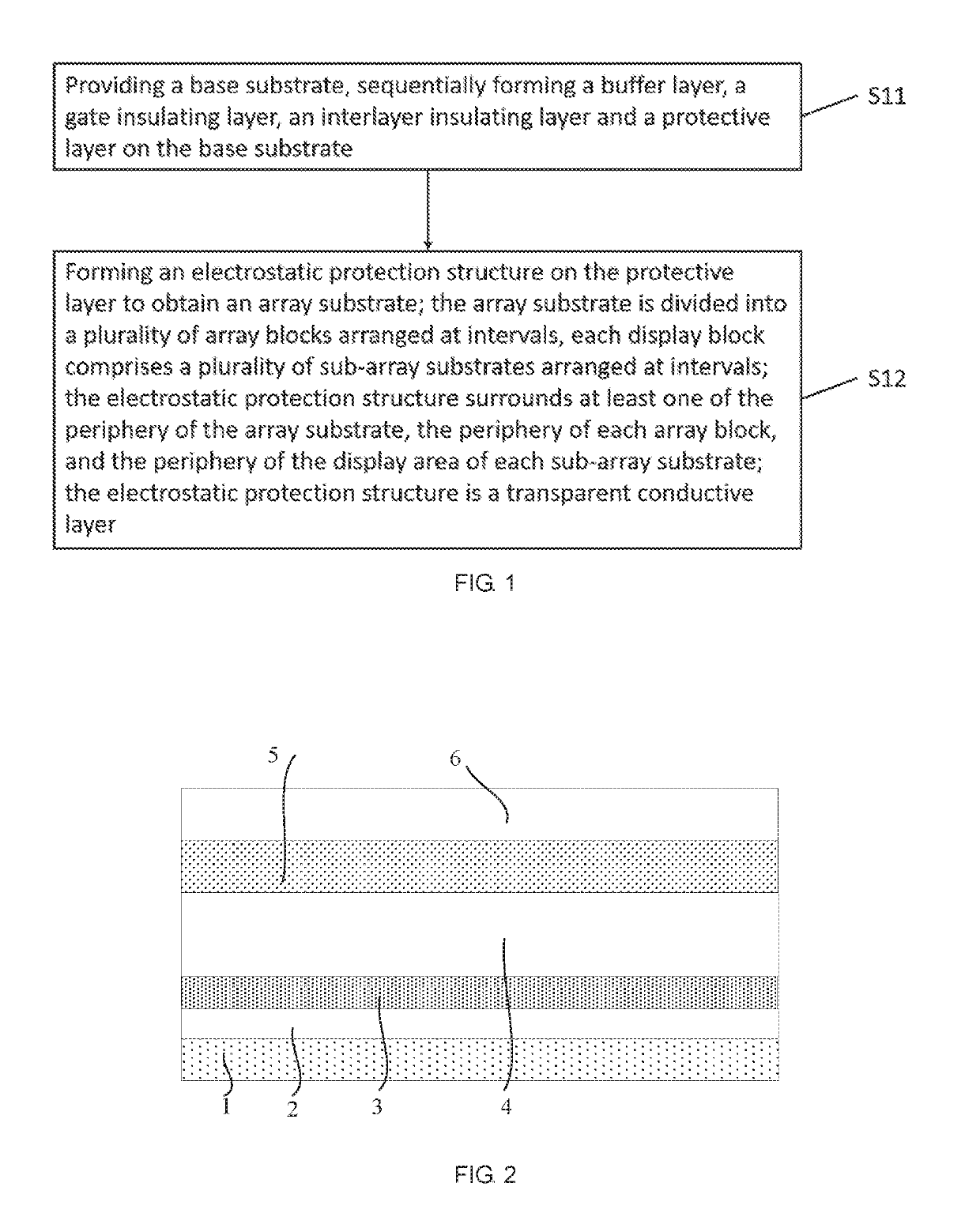
[0036]FIG. 2 is a schematic cross-sectional view of an array substrate with an electrostatic protection structure of the present disclosure, the array substrate is prepared by the method shown in FIG. 1 described above. The structures shown in FIG. 2 all refer to the cross-sectional view of the array substrate in the periphery of the substrate instead of the schematic diagram of the array substrate including the display area. The buffer layer 2, the gate insulating layer 3, the interlayer insulating layer 4 and the protective layer 5 are arranged in the display area of the array substrate. However, the patterned transparent conductive layer 6 is only arranged in the display area of the array substrate and serves as the pixel electrode. In the longitudinal direction, the transparent conductive layer 6 generally does not exist at the periphery of the array substrate, the periphery of the array region and the like. However, in the embodiment of the present disclosure, when a transpare...

embodiment 2

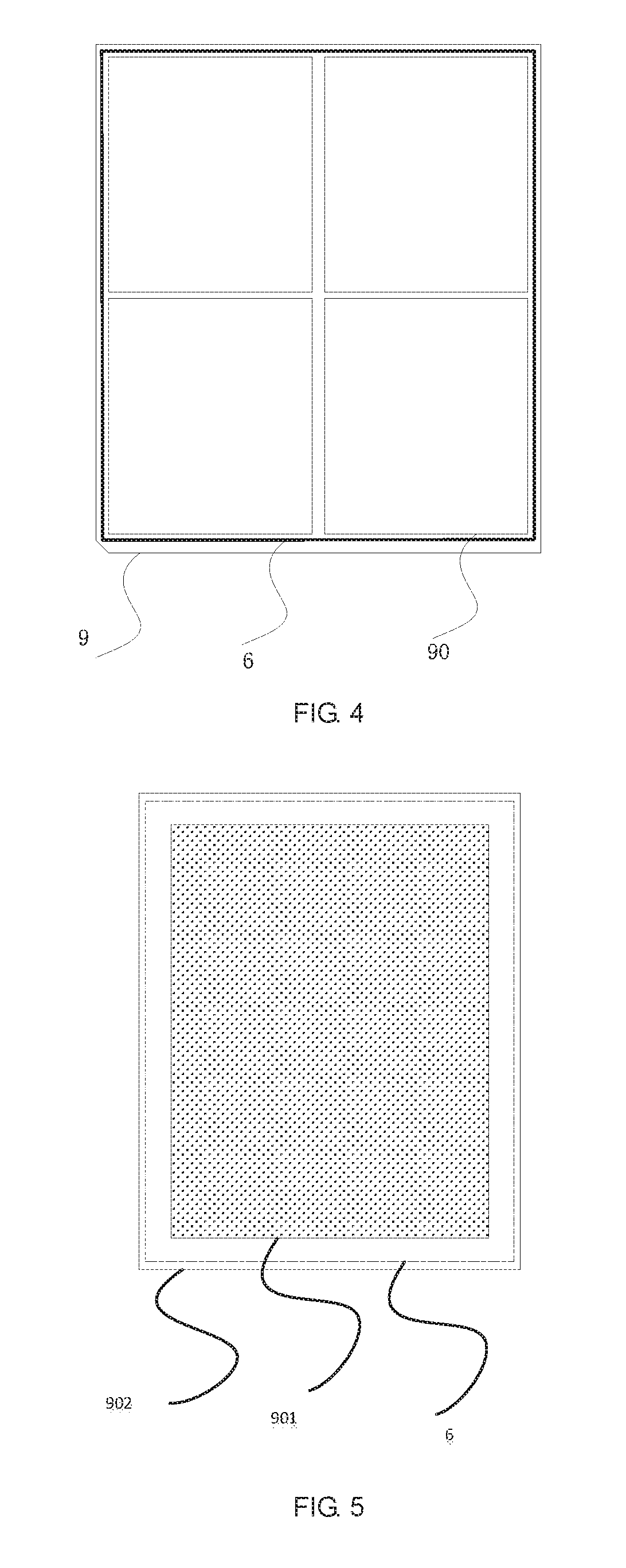
[0040]FIG. 4 is a schematic plan view of an array substrate with an electrostatic protection structure of the present disclosure. In FIG. 4, the electrostatic protection structure 6 is arranged around the periphery of the array substrate 9 (or referred to as the edge and the periphery), and the electrostatic protection structure 6 is a closed ring. In this case, the thickness of the electrostatic protection structure 6 (i.e., the transparent conductive layer 6) may be 200-1000 Å; and its inner diameter (or “width”) may be 2-100 μm.

embodiment 3

[0041]FIG. 5 is a schematic plan view of an array substrate with an electrostatic protection structure of the present disclosure. In FIG. 5, the periphery of the display area 901 of the array substrate (or the periphery and the periphery) of the array substrate is surrounded by the electrostatic protection structure 6. The electrostatic protection structure 6 is an intermittent ring. In this case, the thickness of the electrostatic protection structure 6 (i.e., the transparent conductive layer 6) is 200-1000 Å; and its inner diameter (or “width”) is 2-100 μm. The plurality of sub-array substrates is generally separated by a ring-shaped cutting line 902, so that the array substrate of the later stage is aligned with the color filter substrate up and down and cut along the cutting line to form a plurality of liquid crystal display sub-panels.

[0042]In other embodiments of the present disclosure, the electrostatic protection structure 6 may be arranged around the periphery of the array...


PUM

PropertyMeasurementUnit
inner diameteraaaaaaaaaa
transparentaaaaaaaaaa
transparent conductiveaaaaaaaaaa

Abstract

The present disclosure provides an array substrate, the array substrate includes a plurality of array blocks arranged at intervals, wherein each array block includes a plurality of sub-array substrates arranged at intervals, at least one of a periphery of the array substrate, a periphery of the array block, and a periphery of the display area of the sub-array substrate is arranged with an electrostatic protection structure, the electrostatic protection structure is a transparent metal oxide wire, or a metal wire and a transparent conductive metal oxide wire arranged in layers. The existence of the electrostatic protection structure can effectively shield the outside static electricity. The disclosure also provides a liquid crystal display panel adopting the array substrate.

Description

RELATED APPLICATIONS[0001]This application is a continuation application of PCT Patent Application No. PCT / CN2017 / 114018, filed Nov. 30, 2017, which claims the priority benefit of Chinese Patent Application No. CN 201710771654.8, filed Aug. 31, 2017, which is herein incorporated by reference in its entirety.FIELD OF THE DISCLOSURE[0002]The present disclosure relates to a liquid crystal display technology field, and more particularly to an array substrate and a liquid crystal display panel.BACKGROUND OF THE DISCLOSURE[0003]In recent years, with the development of display technologies, liquid crystal displays (LCDs) are rapidly gaining popularity due to their unique advantages of high image quality, low power consumption and slim body. Among them, the Thin Film Transistor-Liquid Crystal Display (TFT-LCD) is the most commonly used mainstream liquid crystal display and is widely used in electronic settings such as mobile phones and handheld computers.[0004]TFT-LCD display panels are usu...

Claims


Application Information

Patent Timeline
Patent Type & Authority Patents(United States)
IPC IPC(8): G02F1/1362
CPCG02F1/136204G02F1/136286G02F2202/22G02F1/133308G02F1/133334
Inventor LIU, YUANFU
Owner WUHAN CHINA STAR OPTOELECTRONICS TECH CO LTD
Why Eureka
Try Eureka