Substrate comprising an electrical circuit pattern, method and system for providing same

a technology of electrical circuit and substrate, which is applied in the direction of circuit masks, conductive material removal by irradiation, instruments, etc., can solve the problems of generating a lot of heat, unable to bring the optimal solution for high volume roll-to-roll processing, and ablating the metal layer may use a relatively high amount of energy, etc., to achieve no need for expensive (nano)particle inks, large area patterning, and low cos

Active Publication Date: 2019-07-09
NEDERLANDSE ORG VOOR TOEGEPAST-NATUURWETENSCHAPPELIJK ONDERZOEK (TNO)
View PDF24 Cites 0 Cited by
  • Summary
  • Abstract
  • Description
  • Claims
  • Application Information

AI Technical Summary

Benefits of technology

[0006]By selectively irradiating an adhesion between layers, a patterned release of the adhesion can be effectuated. By having a patterned release of adhesion between layers, one or both of said layers can be patterned. By having a release layer adhered on one side of the layer to be patterned, the patterned release can be better controlled. By irradiating through a transparent substrate, the adhesion layer is accessible, e.g. as opposed to irradiation from a side of the adhesion layer covered by material of the layer to be structured, e.g. metal. For example, the light pattern can be projected through transparent material of the stack onto the adhesion layer and / or continuous material layer thereby indirectly heating adjacent layers to causes the release of adhesion. The present methods and system can be used roll to roll in high volume, e.g. by using a flexible substrate and / or release layer. The technique is particularly suitable for providing high quality metal layers and semiconductor layers. This technique does not require time consuming post-treatment steps such as sintering or etching. In contrast with the traditional photo-lithographic process, this method can use a short and high intensity pulse in order to pattern. For example, a flash lamp can be used to cause the release of adhesion. Accordingly, the present method provides improved patterning of structures on substrates.
[0012]By using a decomposable material, an adhesion between the transparent substrate and continuous material layer can be advantageously released. For example, by using a high intensity flash lamp, metal grids can be patterned within milliseconds without the use of etching solutions. Evaporated or sputtered metals on polymer films can be patterned by means of a high intensity light pulse. The light which is not blocked by the mask can generate a lot of heat at the interface of the metal and (polymer) substrate. Due to this heat (e.g. ≥400° C.), the polymer decomposes and the adhesion from the metal to the substrate can decrease significantly. Afterwards, the residual metal is removed by the release liner. Also other ways of releasing an adhesion can be envisaged, e.g. melting.
[0014]To allow a relatively smooth release of the continuous material layer without tearing, preferably the continuous material layer is not too thick. Accordingly, preferably, the continuous material layer has a layer thickness of less than 1000 nm, preferably less than 500 nm, or even thinner.
[0017]Preferably, the mask is resistant to the irradiation light, e.g. does not deteriorate after exposure. For example, in one embodiment, the mask comprises a metal on glass. Suitable metals may include aluminium, chrome, or other metals that on the one hand provide sufficient masking capability and on the other hand sufficient resistance to deterioration.
[0022]Further advantages and applications of the present methods and systems may include suitability for high speed processing, compatibility with roll-to-roll, large area patterning, low cost, no need for expensive (nano)particle inks, cheap RFID antenna structures.

Problems solved by technology

However, as these techniques are relatively slow, they do not bring the optimal solution for high volume roll-to-roll processing.
However, ablating the metal layer may use a relatively high amount energy.
The light which is not blocked by the mask can generate a lot of heat at the interface of the metal and (polymer) substrate.

Method used


Image

  • Substrate comprising an electrical circuit pattern, method and system for providing same
  • Substrate comprising an electrical circuit pattern, method and system for providing same

Examples


Embodiment Construction

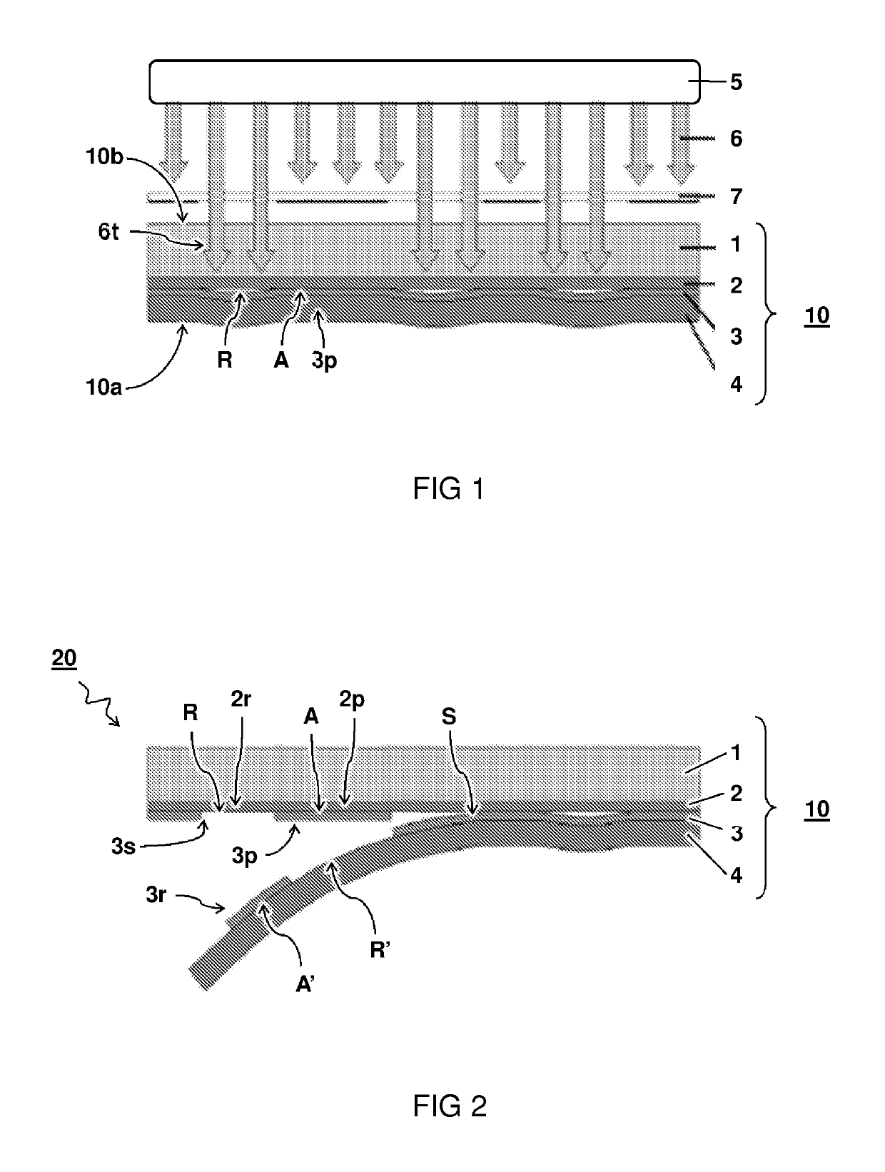
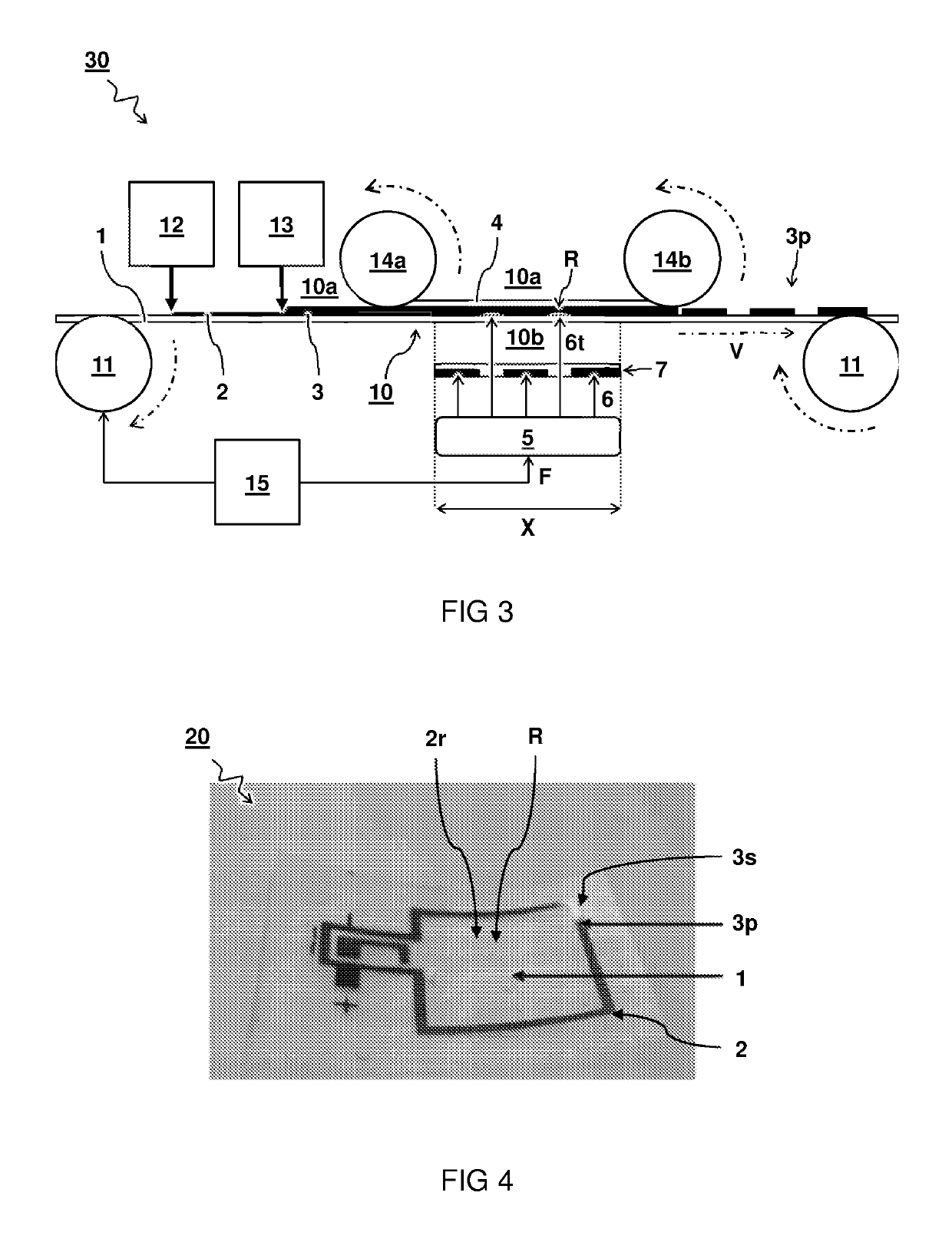
[0028]Unless otherwise defined, all terms (including technical and scientific terms) used herein have the same meaning as commonly understood by one of ordinary skill in the art to which this invention belongs as read in the context of the description and drawings. It will be further understood that terms, such as those defined in commonly used dictionaries, should be interpreted as having a meaning that is consistent with their meaning in the context of the relevant art and will not be interpreted in an idealized or overly formal sense unless expressly so defined herein. In some instances, detailed descriptions of well-known devices and methods may be omitted so as not to obscure the description of the present systems and methods. Terminology used for describing particular embodiments is not intended to be limiting of the invention. As used herein, the singular forms “a”, “an” and “the” are intended to include the plural forms as well, unless the context clearly indicates otherwise...


PUM

PropertyMeasurementUnit
thicknessaaaaaaaaaa
thicknessaaaaaaaaaa
transparentaaaaaaaaaa

Abstract

The present disclosure concerns an electrical circuit pattern on a substrate, as well as a method and system for forming same. In a typical embodiment, a light pattern is projected through a transparent layer to cause a patterned release of adhesion between a continuous material layer and the transparent layer. A release layer adhered to the patterned material layer is pulled off the substrate to separate the material having lower adhesion while leaving the material that was not exposed to form the electrical circuit pattern thereon.

Description

CROSS-REFERENCE TO RELATED APPLICATIONS[0001]This application is a U.S. National Stage application under 35 U.S.C. § 371 of International Application PCT / NL2014 / 050747 (published as WO 2015 / 065181 A1), filed Oct. 29, 2014, which claims priority to Application EP 13190953.3, filed Oct. 30, 2013, and to Application EP 13197496.6, filed Dec. 16, 2013. Benefit of the filing date of each of these prior applications is hereby claimed. Each of these prior applications is hereby incorporated by reference in its entirety.TECHNICAL FIELD AND BACKGROUND[0002]The present disclosure concerns a method and system for forming a patterned structure on a substrate, and the resulting product substrate.[0003]Photolithography and etching processes are often used to pattern thin metal layers on flexible substrates. In photolithography, a polymer can be coated onto the metal film and patterned via UV-light. The metal which is not covered by the polymer is etched away. However, as these techniques are rela...

Claims


Application Information

Patent Timeline
Patent Type & Authority Patents(United States)
IPC IPC(8): G03F7/34H05K1/02G03F7/11G03F7/09H05K3/02B05D3/06H05K3/00
CPCH05K3/027B05D3/06G03F7/092G03F7/11G03F7/34H05K1/0296H05K3/0082G03F7/343H05K2203/0522H05K2201/0108H05K2203/0104G03F7/2002
Inventor HENDRIKS, ROB JACOBSMITS, EDSGER CONSTANT PIETERPERINCHERY, SANDEEP MENONGROEN, PIM
Owner NEDERLANDSE ORG VOOR TOEGEPAST-NATUURWETENSCHAPPELIJK ONDERZOEK (TNO)
Why Eureka
Try Eureka