Method for patterning a lanthanum containing layer

A patterning, barrier layer technology, applied in transistors, electrical components, electrical solid state devices, etc.

Pending Publication Date: 2019-10-08
TAIWAN SEMICON MFG CO LTD
View PDF7 Cites 0 Cited by
  • Summary
  • Abstract
  • Description
  • Claims
  • Application Information

AI Technical Summary

Problems solved by technology

However, these advances have increased the complexity of handling and manufacturing ICs, and in order to achieve these advances, similar developments in IC processing and manufacturing are required

Method used


Image

  • Method for patterning a lanthanum containing layer
  • Method for patterning a lanthanum containing layer
  • Method for patterning a lanthanum containing layer

Examples


Embodiment Construction

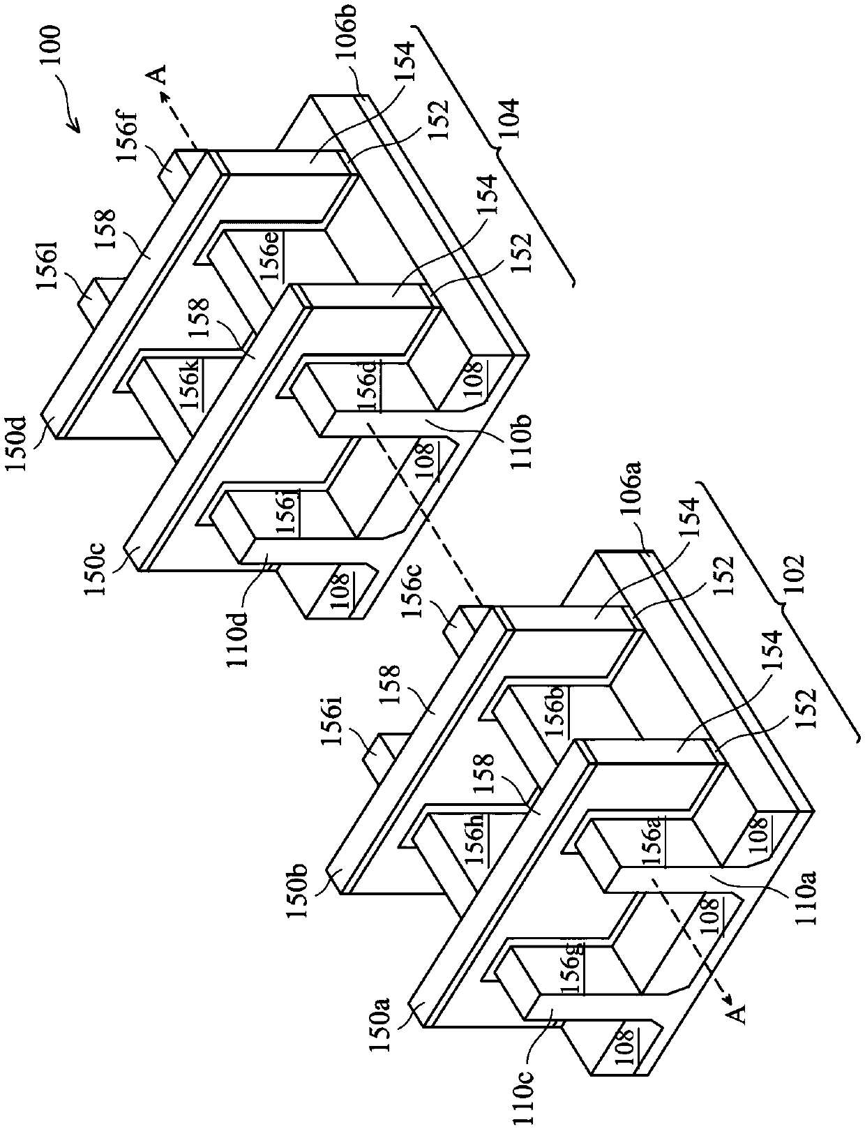
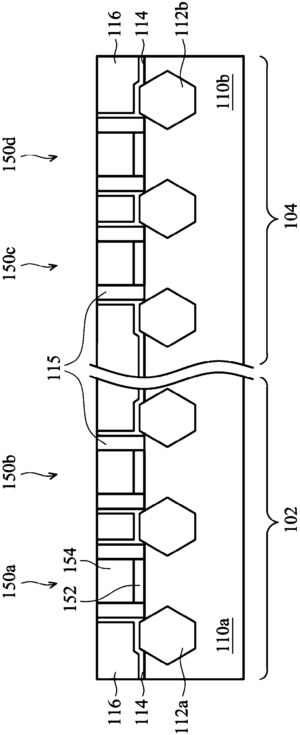
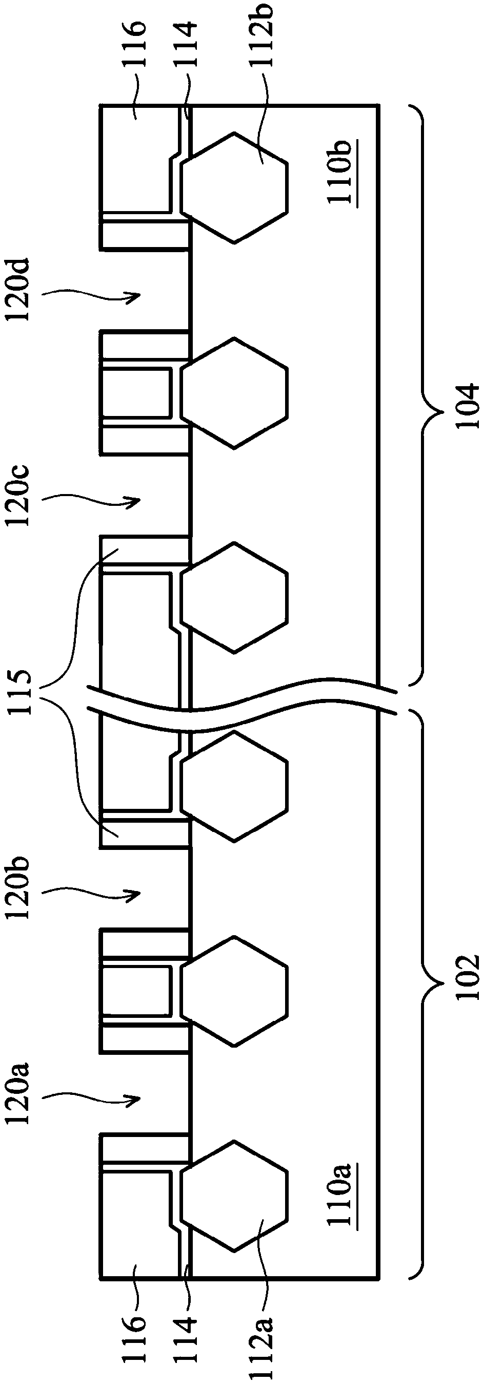
[0011] The following disclosure provides many different embodiments or examples for implementing different features of the provided subject matter. Specific examples of components and arrangements are described below to simplify the invention. Of course, these are only examples and are not intended to limit the invention. For example, in the following description, forming the first member above or on the second member may include an embodiment in which the first member and the second member are directly contacted, and may also include the formation of the first member and the second member. An embodiment in which additional components are used so that the first component and the second component may not directly contact. In addition, the present invention may repeat reference numerals and / or characters in each example. This repetition is for the purpose of simplicity and clarity, and by itself does not indicate the relationship between the various embodiments and / or configura...


PUM

PropertyMeasurementUnit
Thicknessaaaaaaaaaa

Abstract

Embodiments described herein relate to a method for patterning a doping layer, such as a lanthanum containing layer, used to dope a high-k dielectric layer in a gate stack of a FinFET device for threshold voltage tuning. A blocking layer may be formed between the doping layer and a hard mask layer used to pattern the doping layer. In an embodiment, the blocking layer may include or be aluminum oxide (AlOx). The blocking layer can prevent elements from the hard mask layer from diffusing into the doping layer, and thus, can improve reliability of the devices formed. The blocking layer can also improve a patterning process by reducing patterning induced defects. The invention relates to a method for patterning a lanthanum containing layer.

Description

Technical field [0001] Embodiments of the present invention relate to methods for patterning lanthanum-containing layers. Background technique [0002] The semiconductor integrated circuit (IC) industry has experienced rapid growth. Technological advances in IC materials and design have produced multiple generations of ICs, each of which has smaller and more complex circuits than the previous generation. However, these advances have increased the complexity of processing and manufacturing ICs, and to realize these advances, similar developments in IC processing and manufacturing are required. When semiconductor devices such as fin field effect transistors (FinFETs) are scaled down through various technology nodes, various strategies have been adopted to improve device performance, such as the use of high-k dielectric materials and metal gate electrode structures. Summary of the invention [0003] An embodiment of the present invention provides a method for semiconductor processi...

Claims


Application Information

Patent Timeline
IPC IPC(8): H01L21/28H01L27/092H01L29/51
CPCH01L21/2822H01L27/0924H01L27/0922H01L29/517H01L21/823821H01L29/785H01L29/66795H01L29/511H01L21/31144H01L21/31111H01L21/32134H01L21/02321H01L21/3115H01L21/823857H01L21/28185H01L21/02192H01L21/02178H01L21/0228
Inventor 李昆育张惠政张哲豪苏庆煌张文于雄飞
Owner TAIWAN SEMICON MFG CO LTD
Why Eureka
Try Eureka