

Light emitting device package and lighting apparatus
a technology of light emitting devices and lighting devices, which is applied in the direction of basic electric elements, electrical devices, and semiconductor devices, can solve problems such as deteriorating current spreading, and achieve the effects of improving current spreading, high current density, and simplifying manufacturing processes
Active Publication Date: 2019-08-13
SUZHOU LEKIN SEMICON CO LTD
View PDF20 Cites 31 Cited by
- Summary
- Abstract
- Description
- Claims
- Application Information
AI Technical Summary
Benefits of technology
The design achieves improved current density and spreading, simplifies the manufacturing process, and enhances the light emitting device's performance by ensuring uniform carrier injection and protecting the structure from silver migration and impurities.
Problems solved by technology
In a conventional light emitting device package, the carriers supplied into the active layer are not evenly injected, thereby deteriorating current spreading.
Method used
View moreImage
Smart ImageViewing Examples

Examples
Embodiment Construction
[0125]Various embodiments have been described in the best mode for carrying out the invention.
INDUSTRIAL APPLICABILITY
[0126]The light emitting device package according to the embodiment may be used for a display apparatus, an indicator apparatus, and a lighting apparatus such as a lamp, a headlamp, or a street lamp.
Login to View More PUM
 Abstract
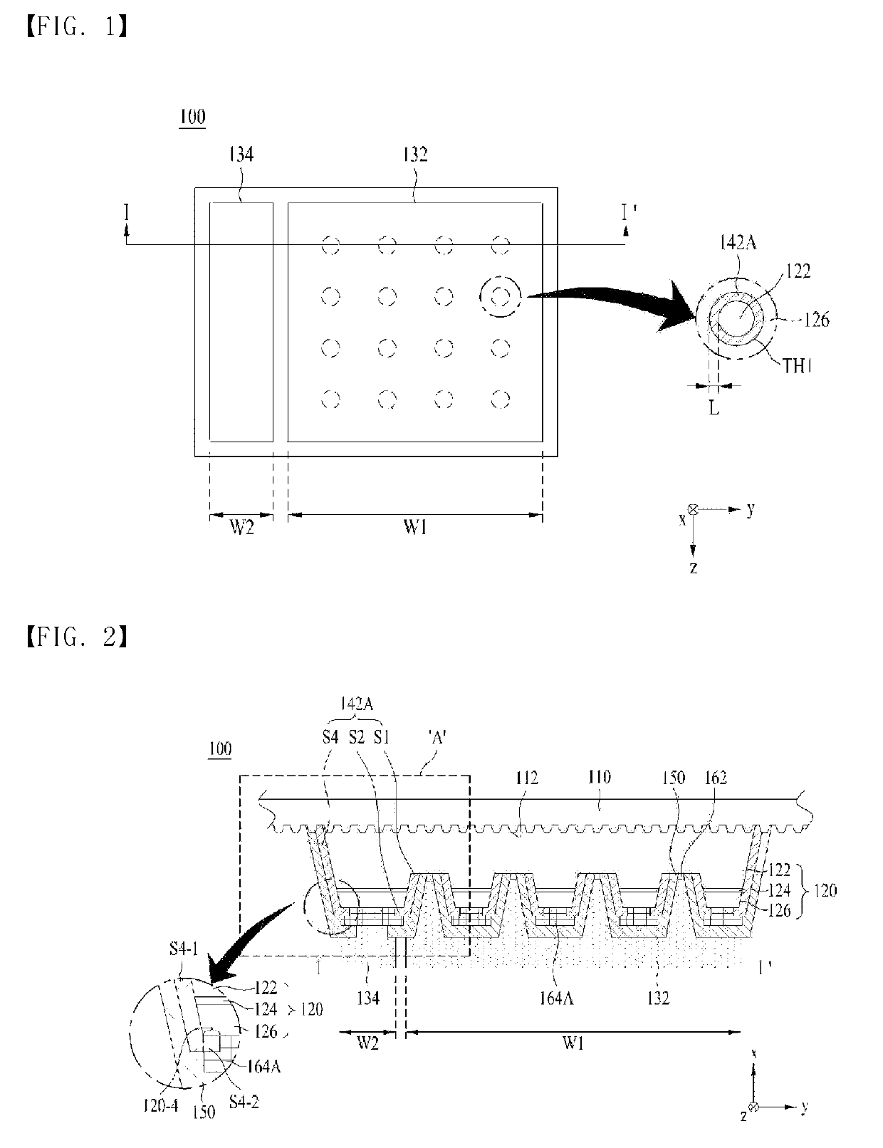
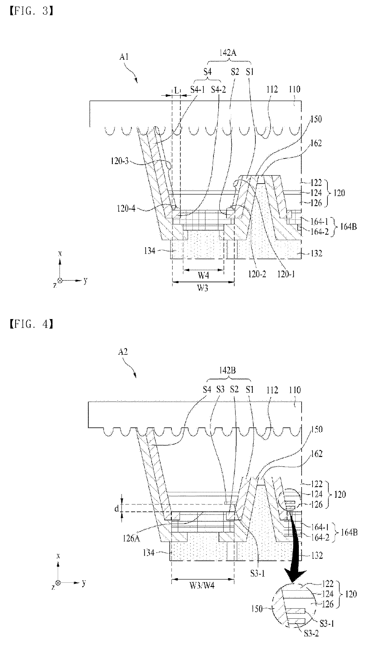
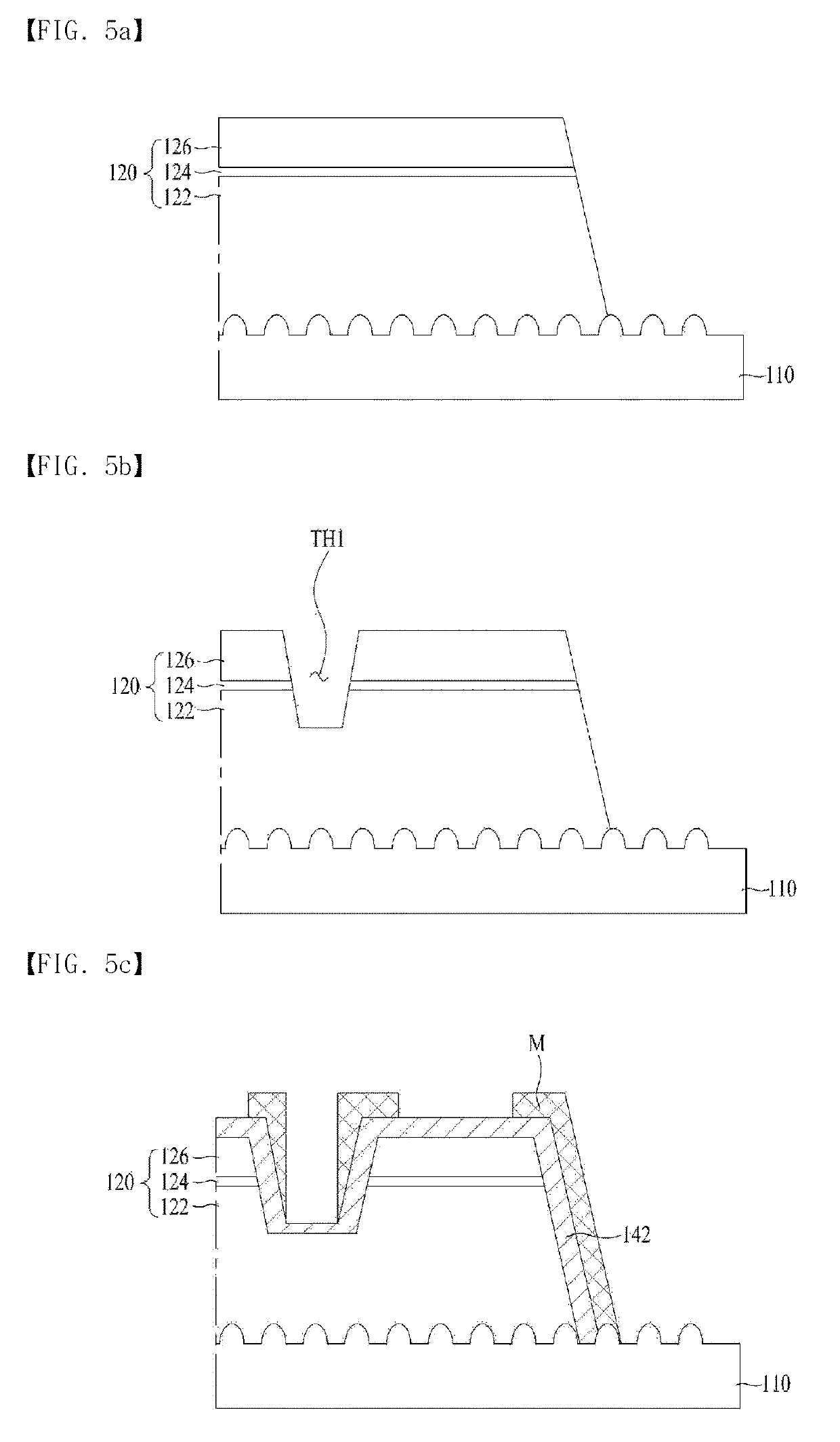
A light emitting device package, according to an embodiment, includes: a substrate; a light emitting structure that is disposed below the substrate and includes a first conductive type semiconductor layer, an active layer, and a second conductive type semiconductor layer; a first bonding pad connected with the first conductive type semiconductor layer while being embedded in a through-hole exposed the first conductive type semiconductor layer by passing through the active layer and the second conductive type semiconductor layer; a second bonding pad that is disposed below the second conductive type semiconductor layer while being spaced apart from the first bonding pad and is connected with the second conductive type semiconductor layer; a first insulation layer disposed on the lateral portion of the light emitting structure in the through-hole and on the lower inner edge of the light emitting structure; and a second insulation layer disposed between the first insulation layer and the first bonding pad in the through-hole.
Description
CROSS REFERENCE TO RELATED APPLICATIONS[0001]This application is the National Phase of PCT International Application No. PCT / KR2016 / 002612, filed on Mar. 16, 2016, which claims priority under 35 U.S.C. 119(a) to Patent Application No. 10-2015-0042659, filed in the Republic of Korea on Mar. 26, 2015, all of which are hereby expressly incorporated by reference into the present application.TECHNICAL FIELD[0002]Embodiments relate to a light emitting device package and lighting apparatus.BACKGROUND ART[0003]A light emitting diode (LED) is a kind of semiconductor device that converts electricity into infrared rays or light using the properties of a compound semiconductor to transmit or receive a signal or that is used as a light source.[0004]Group III-V nitride semiconductors have attracted attention as a core material of a light emitting device, such as a light emitting diode (LED) or a laser diode (LD), thanks to the physical and chemical properties thereof.[0005]The light emitting diod...
Claims
Login to View More Application Information
Patent Timeline
 Patent Type & AuthorityPatents(United States)
IPC IPC(8): H01L33/44H01L33/62H01L33/38H01L33/32H01L33/14H01L33/40
CPCH01L33/44H01L33/382H01L33/62H01L33/405H01L33/145H01L33/32H01L33/14
InventorSEO, JAE WONKIM, HOE JUNYIM, BUM JINHONG, JUN HEE
OwnerSUZHOU LEKIN SEMICON CO LTD