Method of manufacturing light distribution member with shielded individual transmissive pieces and light-shielding frame, method of manufacturing light emitting device having light distribution member, light distribution member, and light emitting device

a technology of transmitsive pieces and light-shielding frames, which is applied in the direction of semiconductor devices, solid-state devices, lighting and heating apparatuses, etc., can solve the problems of requiring a certain amount of space between wavelength conversion members, light leakage from wavelength conversion members provided, and the effect of reducing emission efficiency

Active Publication Date: 2019-09-17
NICHIA CORP
View PDF42 Cites 0 Cited by
  • Summary
  • Abstract
  • Description
  • Claims
  • Application Information

AI Technical Summary

Benefits of technology

[0027]Disclosed herein is a light distribution member with which light leakage can be prevented between transmissive pieces provided to lit and unlit light emitting elements without decreasing emission efficiency, as well as a method for manufacturing the light distribution member and a light emitting device that have the same effect.

Problems solved by technology

With a light emitting device such as this, however, if there is an unlit light emitting element adjacent to a lit light emitting element when the lighting of the plurality of light emitting elements is controlled independently for each one, there may be light leakage from the wavelength conversion member provided to the lit light emitting element, and the wavelength conversion member provided to the unlit light emitting element may emit a tiny amount of light.
However, forming the reflective resin requires a certain amount of space between wavelength conversion members.
Also, when a light-shielding film composed of a metal film or a dielectric multilayer film is formed on the side surface of a flat wavelength conversion member, an adequate light shielding or reflecting effect cannot be obtained if the side surface is bumpy.
Furthermore, it is not easy to control the film thickness in forming a metal film or a dielectric multilayer film on the side surface, and it is difficult to form the film evenly on the side surface.

Method used


Image

  • Method of manufacturing light distribution member with shielded individual transmissive pieces and light-shielding frame, method of manufacturing light emitting device having light distribution member, light distribution member, and light emitting device
  • Method of manufacturing light distribution member with shielded individual transmissive pieces and light-shielding frame, method of manufacturing light emitting device having light distribution member, light distribution member, and light emitting device
  • Method of manufacturing light distribution member with shielded individual transmissive pieces and light-shielding frame, method of manufacturing light emitting device having light distribution member, light distribution member, and light emitting device

Examples


embodiment 1

anufacturing Light Distribution Members

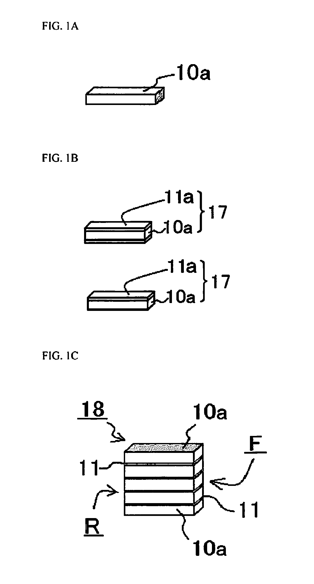
[0122]With a method for manufacturing a light distribution members in this Embodiment 1, first, a transmissive plate 10a is prepared as shown in FIG. 1A. This transmissive plate 10a is obtained by mixing a YAG phosphor in an amount of about 10 wt % into a glass material, sintering this mixture, and cutting the resulting large-sized YAG plate to the proper size.

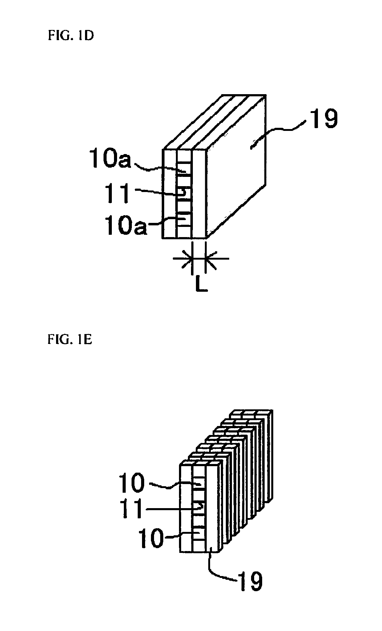
[0123]As shown in FIG. 1B, a first light-shielding film 11a composed of a metal multilayer film (titanium, platinum, and gold, in that order starting from the transmissive plate side) is successively formed by sputtering in respective thicknesses of 100 nm, 200 nm, and 500 nm (for a total thickness of 800 nm) on only one side of this transmissive plate 10a, to form a first light-shielding film member 17. Two of these first light-shielding film members 17 are formed. Also, a plurality of first light-shielding film members 17 in which the first light-shielding film 11a is formed on both sid...

embodiment 2

anufacturing Light Emitting Device

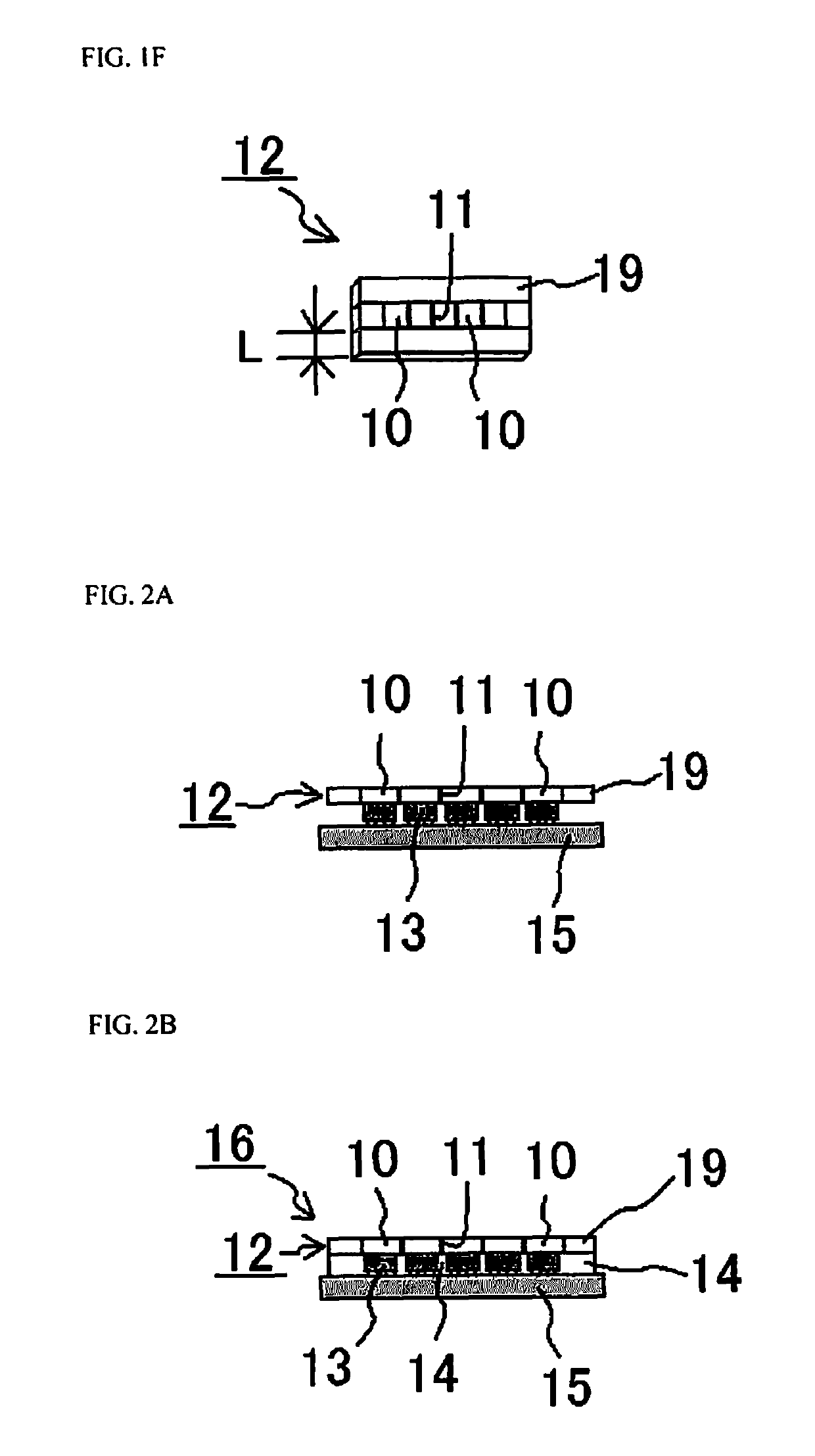
[0131]With a method for manufacturing a light emitting device in Embodiment 2, as shown in FIG. 2A, light emitting elements 13 are disposed corresponding to one light distribution member 12 obtained in Embodiment 1. That is, five light emitting elements 13 are disposed spaced apart and corresponding to the respective positions of the transmissive pieces 10 segmented by the light shield parts 11 of the light distribution member 12.

[0132]The light emitting elements 13 are mounted on a support substrate 15 of which a wiring pattern has been formed on the upper surface in a face-down form in a row by soldering. The light distribution member 12 is then fixed with an adhesive member to the light extract surface side of the light emitting elements 13 thus disposed.

[0133]Then, as shown in FIG. 2B, a light emitting device 16 is formed by disposing reflective member 14 that include a silicone resin containing about 50% titanium dioxide so as to be disposed be...

embodiment 3

anufacturing Light Distribution Members

[0137]With a method for manufacturing light distribution members in Embodiment 3 is substantially the same as the method for manufacturing light distribution members in Embodiment 1, except that the transmissive plates are cut in two directions.

[0138]First, a transmissive plate 20a is prepared as shown in FIG. 3A.

[0139]Then, as shown in FIG. 3B, a first light-shielding film 21a composed of a multilayer metal film is formed on the surface of this transmissive plate 20a to form a first light-shielding film member 27. The width of the first light-shielding film member 27 in this case shall be about 200 μm, for example. The width referred to here indicates the length W in the lateral direction in FIG. 3B.

[0140]Next as shown in FIG. 3C, for example, five of the first light-shielding film members 27 is successively joined at normal temperature so that the first light-shielding films 21a are opposite, thereby forming a first joined body 28 that is lam...


PUM


Abstract

A light distribution member includes a body and a light-shielding frame. The body includes a plurality of transmissive pieces and a plurality of light shield parts each interposed between adjacent ones of the transmissive pieces. Each of the transmissive pieces is made of a phosphor or made of a sinter of a phosphor and a binder composed of an inorganic substance. The light-shielding frame is provided so as to surround an outer edge periphery of the body. The light-shielding frame is made of a ceramic. The light distribution member contains substantially no organic substance inside the light-shielding frame.

Description

CROSS-REFERENCE TO RELATED APPLICATIONS[0001]This application claims priority to Japanese Patent Applications No. 2015-099985 and No. 2016-092633 filed on May 15, 2015 and May 2, 2016. The entire disclosures of Japanese Patent Applications No. 2015-099985 and No. 2016-092633 are hereby incorporated herein by reference.BACKGROUND[0002]1. Technical Field[0003]The present disclosure relates to a method of manufacturing a light distribution member, a method of manufacturing a light emitting device, a light distribution member, and a light emitting device.[0004]2. Description of Related Art[0005]A light emitting device equipped with a plurality of light emitting diodes or other such light emitting elements has been used in the past as a light source utilized in automotive headlights. With this light emitting device used in automotive headlights, a plurality of light emitting elements are arranged on a substrate, and wavelength conversion members that contain a phosphor are disposed on th...

Claims


Application Information

Patent Timeline
Patent Type & Authority Patents(United States)
IPC IPC(8): F21V11/06F21V7/00F21V13/08F21V11/16H01L25/075H01L33/50H01L33/60H01L33/64
CPCH01L25/0753F21V7/0083H01L33/60F21V11/16H01L33/505H01L2933/0041H01L2933/0058H01L33/644H01L33/507H01L33/501H01L33/58
Inventor WAKAMATSU, DAIICHIKAWA, MASATSUGUSANO, MASAHIKO
Owner NICHIA CORP
Why Eureka
Try Eureka