Display module and display device

a display module and display device technology, applied in the field of display, can solve the problems of poor contact between the cof and the liquid crystal panel or the printed circuit board, cumbersome and time-consuming operation, and inconvenient operation

Active Publication Date: 2019-10-15
BOE TECH GRP CO LTD
View PDF30 Cites 0 Cited by
  • Summary
  • Abstract
  • Description
  • Claims
  • Application Information

AI Technical Summary

Benefits of technology

[0005]As consumers' requirements to image quality of the display device are becoming more demanding, an amount of system signals and power information handled by the chip of a thin film transistor liquid crystal display (referred to as TFT-LCD) is also becoming even larger, and an increase in loading capacity necessarily brings about more heat generation. Therefore, a good heat dissipation is needed. Solutions which are generally adopted in the conventional heat dissipation of the chip lie in that: a heat dissipation patch covering the chip is attached to the COF so as to cool the chip.

Problems solved by technology

The conventional technology has the drawback lying in that, since both the COF and the heat dissipation patch have certain flexibility, it is necessary to keep the COF and the heat dissipation patch to be flattened and smooth, when the heat dissipation patch is bonded to the COF.
Such an operation is very inconvenient.
In particular, a large-size display module has dozens of COFs which makes the operation cumbersome and time-consuming.
In addition, after the COF and the heat dissipation patch are bonded together, if the heat dissipation patch needs to be removed, the COF and the heat dissipation patch tends to pull each other due to a relative large bonding force existing therebetween, so that there is a poor contact between the COF and the liquid crystal panel or the printed circuit board.
However, if the COF and the heat dissipation patch are not firmly bonded to each other, a gap may thus be formed therebetween, resulting in that the heat dissipation effect will be greatly compromised.
For a non-TFT-LCD display product, such as an OLED (Organic Light-Emitting Diode) product, the heat dissipation structure of the chip thereof is similar to that described above, thus similar technical problems to those described above may also exist.

Method used


Image

  • Display module and display device
  • Display module and display device
  • Display module and display device

Examples


Embodiment Construction

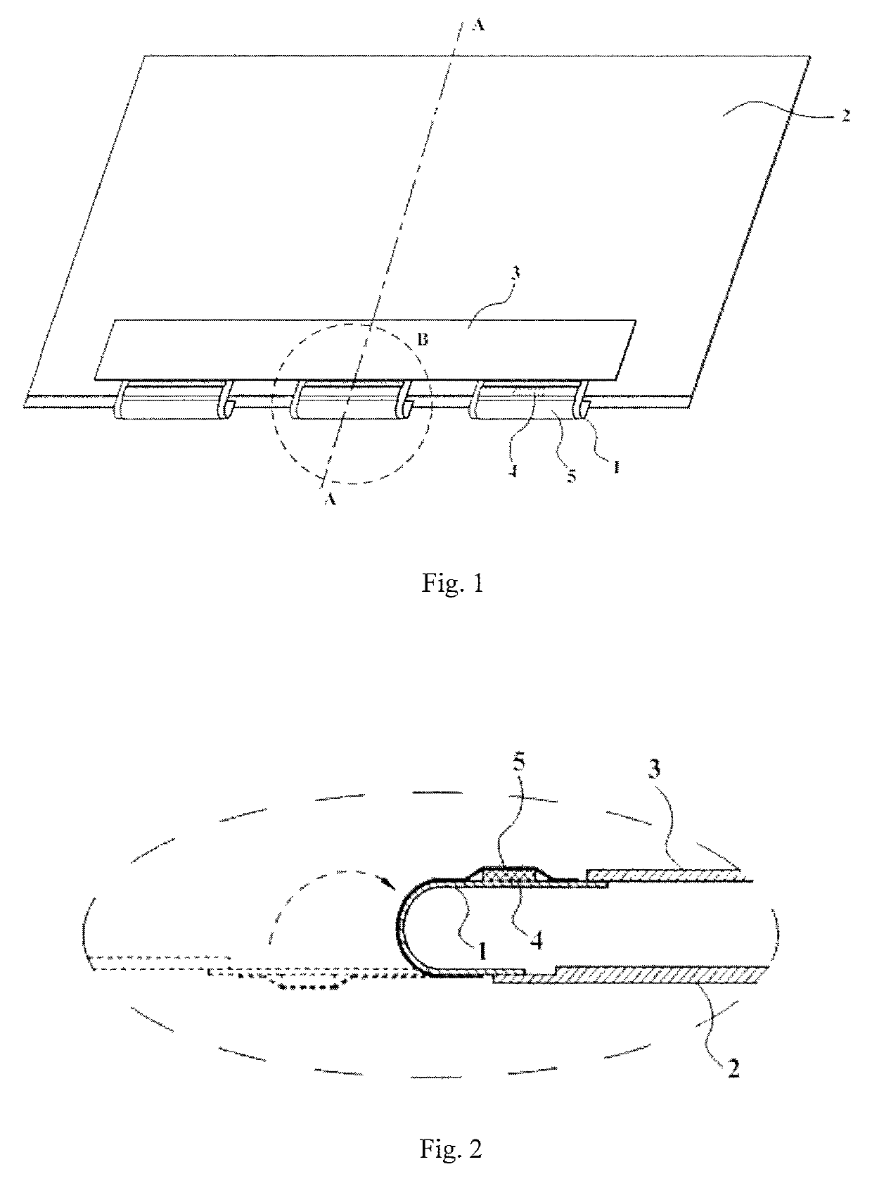
[0027]FIG. 1 is a schematic view of a heat dissipation structure of a chip of a conventional display module and FIG. 2 is an enlarged sectional view at B in FIG. 1, respectively. As shown in FIG. 1 and FIG. 2, in a conventional TFT-LCD, a chip-on-film (referred to as COF) 1 is connected between a liquid crystal panel 2 and a printed circuit board 3, and is bent towards a backside of a back plate of a back light module from a periphery of the liquid crystal panel 2 (the backlight module, and a cover plate as set forth hereinafter are not shown), a chip 4 is packaged on the COF 1, and the cover plate fixed on the back side of the back plate of the backlight module covers and protects the printed circuit board 3 and chip 4. A heat dissipation patch 5 covering the chip 4 is attached to the COF 1 to cool the chip 4.

[0028]The present disclosure provides a display module and a display device for the sake of improving assembly convenience of the display module, enhancing the heat dissipatio...


PUM

PropertyMeasurementUnit
thermal conductiveaaaaaaaaaa
thermal-aaaaaaaaaa
thicknessaaaaaaaaaa

Abstract

The present disclosure relates to a display module and a display device. The display module includes a display panel, at least one chip-on-film, a printed circuit board and a cover plate, wherein: the printed circuit board is located on a back side of the display panel; one end of the chip-on-film is connected with the display panel, the other end of the chip-on-film is bent towards the back side of the display panel and is connected with a printed circuit board, with a chip being packaged in a portion of the chip-on-film which is bent towards the back side of the display panel; the cover plate is located on the back side of the printed circuit board and covers the same; the cover plate is provided with thermal conductive blocks which are in thermal contact with the chip at each location of the cover plate corresponding to one of the chip-on-film respectively. The display module according to the present disclosure improves the assembly convenience of the display module, improves the heat dissipation performance of the chip, and further improves the product quality of the display device.

Description

CROSS-REFERENCE TO RELATED APPLICATION[0001]This application is a Section 371 National Stage Application of International Application No. PCT / CN2017 / 079442, filed Apr. 5, 2017, and published as WO 2017 / 177848 A1 on Oct. 19, 2017, and claims the benefit of Chinese Patent Application No. 201610228560.1 filed on Apr. 13, 2016 in the State Intellectual Property Office of China, the whole disclosure of which are incorporated herein by reference.BACKGROUND OF THE INVENTION[0002]Field of the Invention[0003]The present disclosure relates to the technical field of display, and in particular to a display module and a display device.[0004]Description of the Related Art[0005]As consumers' requirements to image quality of the display device are becoming more demanding, an amount of system signals and power information handled by the chip of a thin film transistor liquid crystal display (referred to as TFT-LCD) is also becoming even larger, and an increase in loading capacity necessarily brings a...

Claims


Application Information

Patent Timeline
Patent Type & Authority Patents(United States)
IPC IPC(8): G02F1/1333H05K1/02H05K7/20G02F1/133F21V29/70
CPCF21V29/70F21V29/71G02F1/133G02F1/133385G02F1/13452H05K7/20454H05K7/20963G02F1/1333G02F1/133308H05K1/0203H05K7/2039
Inventor WANG, ZIFENGREN, YANHU, NANNANCAO, LEILIN, SHE
Owner BOE TECH GRP CO LTD
Why Eureka
Try Eureka