Unlock instant, AI-driven research and patent intelligence for your innovation.

Multiple concurrent modulation schemes in a memory system

Active Publication Date: 2019-10-15
MICRON TECH INC
View PDF51 Cites 0 Cited by
  • Summary
  • Abstract
  • Description
  • Claims
  • Application Information

AI Technical Summary

Benefits of technology

The present patent application claims priority to a provisional patent application filed in October 2017 and describes a memory device that supports multiple concurrent modulation schemes. This means that the device can use multiple methods to improve its performance and reliability. The patent describes various circuits and processes that can be used to achieve this goal. The technical effect of this patent is to improve the performance and reliability of memory devices by using multiple concurrent modulation schemes.

Problems solved by technology

Memory devices may be volatile or non-volatile.
Volatile memory devices, e.g., DRAM, may lose their stored state over time unless they are periodically refreshed by an external power source.

Method used


Image

  • Multiple concurrent modulation schemes in a memory system
  • Multiple concurrent modulation schemes in a memory system
  • Multiple concurrent modulation schemes in a memory system

Examples


Embodiment Construction

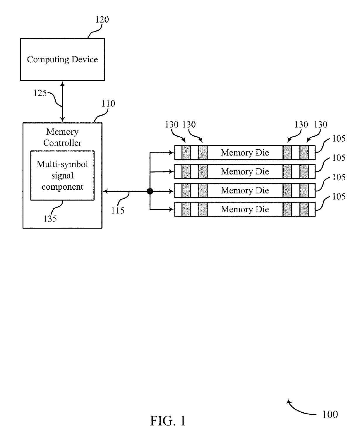
[0031]Some memory devices may transfer data across a number of channels in a memory device using different signaling techniques. For example, one signaling example may include using a signal modulated using a first modulation scheme having multiple levels (e.g., at least three levels). Such signaling may be configured to increase a data transfer rate without increasing the frequency of data transfer and / or a transmit power of the communicated data. Examples of different signaling techniques may include, among others, non-return-to-zero (NRZ) signaling and pulse amplitude modulation (PAM) signaling.

[0032]In some examples, a memory controller may be configured to communicate a first and second signal type to a memory die. The signals may be communicated through a first and second signal path, respectively, and may each be modulated using a different modulation scheme. Using multiple modulation schemes may result in improved read and write speeds of a memory array. To communicate the s...


PUM


Abstract

Methods, systems, and devices for multiple concurrent modulation schemes in a memory system are described. Techniques are provided herein to communicate data using a modulation scheme having at least three levels and using a modulation scheme having at least two levels within a common system or memory device. Such communication with multiple modulation schemes may be concurrent. The modulated data may be communicated to a memory die through distinct signal paths that may correspond to a particular modulation scheme. An example of a modulation scheme having at least three levels may be pulse amplitude modulation (PAM) and an example of a modulation scheme having at least two levels may be non-return-to-zero (NRZ).

Description

CROSS REFERENCE[0001]The present application for patent claims the benefit of and claims priority to U.S. Provisional Patent Application No. 62 / 567,018 by Hasbun et al., entitled “Multiple Concurrent Modulation Schemes in a Memory System,” filed Oct. 2, 2017, assigned to the assignee hereof, which is expressly incorporated herein by reference.BACKGROUND[0002]The following relates generally to using signaling in a memory device. Memory devices are widely used to store information related to various electronic devices such as computers, wireless communication devices, cameras, digital displays, and the like. Information is stored by programing different states of a memory cell.[0003]Various types of memory devices exist, including magnetic hard disks, random access memory (RAM), read only memory (ROM), dynamic RAM (DRAM), synchronous dynamic RAM (SDRAM), ferroelectric RAM (FeRAM), magnetic RAM (MRAM), resistive RAM (RRAM), flash memory, phase change memory (PCM), and others. Memory de...

Claims


Application Information

Patent Timeline
IPC IPC(8): G11C7/10G11C11/22G06F13/42G06F1/3234G11C11/4093
CPCG11C7/1006G11C7/1057G11C7/1084G11C7/22G11C7/1048G11C7/1051G11C7/1078Y02D10/00G06F13/4234G06F13/1689G06F13/1684G06F3/0658G06F3/061G06F3/0614G11C5/06H03K7/02G06F1/3234G11C11/4093G06F13/42G11C11/2253G11C11/221G11C11/2273
Inventor HASBUN, ROBERT NASRYHOLLIS, TIMOTHY M.WRIGHT, JEFFREY P.GANS, DEAN D.
Owner MICRON TECH INC
Features
  • R&D
  • Intellectual Property
  • Life Sciences
  • Materials
  • Tech Scout
  • Unparalleled Data Quality
  • Higher Quality Content
  • 60% Fewer Hallucinations
Learn More