Method for the electrical passivation of electrode arrays and/or conductive paths in general, and a method for producing stretchable electrode arrays and/or stretchable conductive paths in general

a technology of conductive paths and electrode arrays, applied in the direction of dielectric characteristics, diagnostic recording/measuring, therapy, etc., can solve the problems of damage to the conductors underneath, cost arising and complexity of machinery and equipment needed to carry out the above method, and the effect of several drawbacks

Active Publication Date: 2019-10-15
ECOLE POLYTECHNIQUE FEDERALE DE LAUSANNE (EPFL)
View PDF5 Cites 0 Cited by
  • Summary
  • Abstract
  • Description
  • Claims
  • Application Information

AI Technical Summary

Benefits of technology

[0020]It is therefore an object of the present invention that of overcoming or at least reducing the drawbacks affecting the prior art passivation and / or encapsulation methods.
[0021]In particular, an object of the present invention is that of proposing a method for passivating and / or encapsulating conductive paths or electrical circuits in general, adapted to be carried out at reduced and / or contained costs and without any need of using complex and / or expensive and / or bulky machinery or equipment and possibly without using liquid etchants; to the contrary, according to the present invention, the encapsulating process shall be a completely “dry” process.
[0022]Moreover, a further goal of the present invention is that of proposing an encapsulation and / or passivation method according to which chemical or physical agents like for instance solvents and / or etchants may be avoided.
[0031]The present invention is based on the consideration that the drawbacks affecting the passivation or encapsulation methods according to the prior art (at least those relating to the risk of damaging the conductors due to exposition to or contact with the etchants used for opening the vias into the passivation layer) may be efficiently and conveniently overcome by forming the passivation layer (comprising the through vias) separately from the electrodes or conductors array(s) and by bonding the previously prepared passivation layer to the conductors (or the layer or substrate underneath) once the vias have been adequately aligned with those portions of the conductors or conductive paths (in general the contact pads), which do not need to be encapsulated but have to stay uncovered or exposed. In this way, independently thereon which solution is used for forming the through vias, no risks arise to damage the conductors during formation of the vias. Moreover, expensive steps and machinery such as, for instance, those for photolithography, lamination, spraying, chemical vapour deposition, dry or whet etching or the like may be avoided.
[0033]A further consideration on which the present invention is based relates to the fact that further advantages arise by forming the passivation layer (with through vias) on a soft substrate other than the substrate which supports the conductors; in fact, with a soft substrate or layer supporting the passivation layer, the thickness of the passivation layer may be selected according to the needs and / or circumstances (the passivation layer may be as thin as needed), thus being the passivation layer particularly suitable for passivating very thin stretchable electrode arrays. Moreover, the vias may be easily formed according to any solution, for instance even using a very simple mechanical (punching) tool.
[0034]Still a further consideration on which the present invention is based relates to the fact that further advantages may be obtained when the passivation layer is formed by (comprises) two layers, namely a first and a second passivation layer (eventually with a release layer therebetween); in fact, the upper passivation layer may be used as a masking layer for filling the vias with conductive material once the entire passivation layer (comprising first and second passivation layers) has been placed on the conductors and the lower passivation layer has been bonded to same. In this way, by removing the upper passivation layer, conductive material eventually lying on same is removed too, thus obtaining an adequately passivated circuit or conductive path, wherein the through vias in the passivation layer are adequately filled with conductive material.

Problems solved by technology

However, even if said lithography and / or etching methods have revealed to be quite convenient for several reasons, (very small and / or precise vias may be open with a predefined shape and at predefined positions), said methods are still affected by several drawbacks and / or disadvantages.
One of said drawbacks relates in particular to the costs arising and to the complexity of the machinery and equipment needed for carrying out the above methods.
Moreover, a further drawback relates to the fact that organic solvents or even very aggressive physical or chemical etchants have to be used, which however can lead to damages of the conductors underneath or even, in the worst cases, to the partial or even complete removal of said conductors.
Moreover, the chemicals etchants may also damage the carrier substrate or be absorbed by the substrate material (especially if it is a polymer).
In particular, avoiding the risk of damaging the conductors and / or substrate underneath represents an important challenge in the field of fabrication of elastic or stretchable electrode array, wherein the substrate is an elastomer and the thickness of the conductors or conductive paths amounts to a few, typically 1 to 100 nm.
It appears therefore clearly from the above that encapsulating the electrodes (whilst leaving the connector pads exposed) represents a difficult task due to the mandatory need of avoiding any risk of damaging the electrodes and / or connector pads.

Method used


Image

  • Method for the electrical passivation of electrode arrays and/or conductive paths in general, and a method for producing stretchable electrode arrays and/or stretchable conductive paths in general
  • Method for the electrical passivation of electrode arrays and/or conductive paths in general, and a method for producing stretchable electrode arrays and/or stretchable conductive paths in general
  • Method for the electrical passivation of electrode arrays and/or conductive paths in general, and a method for producing stretchable electrode arrays and/or stretchable conductive paths in general

Examples


Embodiment Construction

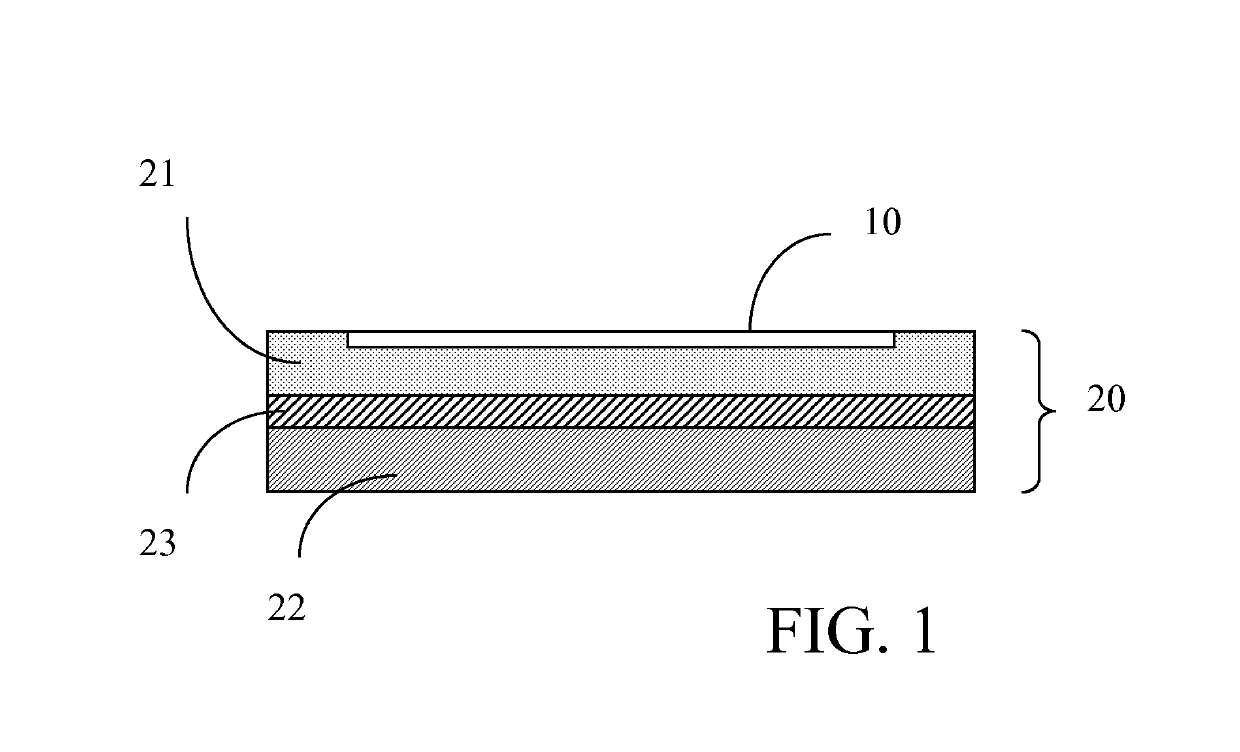
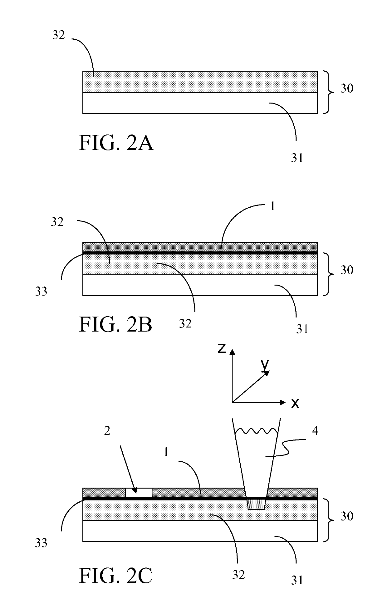
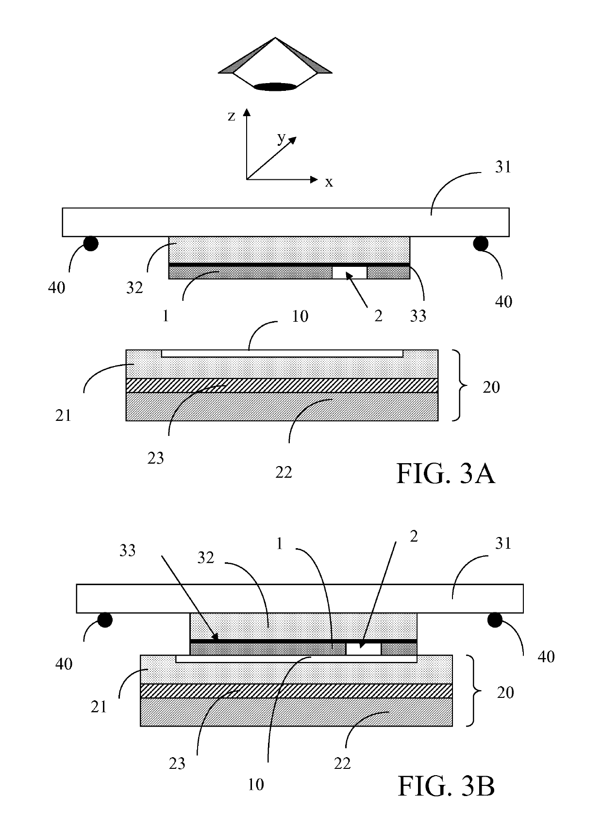
[0062]In FIGS. 1 to 4, the reference 10 identifies an electrode array, for instance a microelectrode array comprising at least one conductive path; in the following, for the sake of convenience and clarity, the electrode array 10 will be eventually simply referred to as a “conductive path” or “array of conductive paths”. Said conductive paths 10 may be formed according to any of the methods known in the art such as, for instance, metal deposition of a continuous metal film ad etching, metal evaporation or the like. Since the particular method used for forming the conductive path 10 does not fall within the scope of the present invention, detailed description of same is omitted for the sake of conciseness.

[0063]The thickness of the layer carrying the ‘array of conductive paths’ is determined by the application requirements with thickness limitations of known methods for depositing such layers. By way of example for silicone rubber, the thickness of the layer can vary between 1 μm to ...


PUM

PropertyMeasurementUnit
viscosityaaaaaaaaaa
thicknessaaaaaaaaaa
thickaaaaaaaaaa

Abstract

A method produces a conductive paste comprising 15-20% by weight of PDMS and 80-85% by weight of metallic micro-nano particles, wherein the conductive paste is obtained by repeated addition of singular doses of PDMS to a heptane diluted PDMS low viscosity liquid containing the metallic micro-nano particles, wherein the heptane fraction is allowed to evaporate after addition of each of the singular doses of PDMS. A method forms a conductive path on a support layer, wherein the conductive path is encapsulated by an encapsulation layer comprising at least one via through which at least one portion of the conductive path is exposed, the method comprising filling the at least one via with the conductive paste.

Description

BACKGROUND[0001]Technical Field[0002]The present invention belongs to the field of electrode arrays and / or conductive paths or circuits in general. In particular, the present invention relates to a method for conveniently passivating and / or encapsulating electrode arrays or conductive paths in general, as well as to a method for producing and / or fabricating electrode arrays and / or conductive paths in general. Still in more detail, the present invention relates to a method for conveniently passivating stretchable electrode arrays, as well as to a method for producing and / or fabricating stretchable electrode arrays. According to the present invention there is further provided a method for producing a conductive material suitable for manufacturing electrode arrays or conductive paths in general, in particular for manufacturing stretchable electrode arrays, along with a conductive material produced according to the method and an electrode array or conductive path produced by using said ...

Claims


Application Information

Patent Timeline
Patent Type & Authority Patents(United States)
IPC IPC(8): H01K3/10H05K1/09H05K3/00A61B5/04A61N1/04H05K1/02H01B1/22H05K3/12H05K3/28H05K3/40H01L23/498A61N1/05H01L23/538
CPCA61B2562/046A61B2562/125A61N1/0476A61N1/0531A61N1/0551H05K1/0283H05K2201/0133H01B1/22H01L2924/0002H05K3/4069H05K2201/0108H05K2203/0537H05K2203/1322Y10T29/49165H05K3/28H05K2201/0257A61B5/24A61B5/388H01L2924/00H01L23/4985H01L23/5387H05K1/0272H05K3/284H05K2201/0314H05K1/092H05K3/005H05K3/007H05K3/12H05K3/4038H05K2201/0215H05K2201/0329H05K2203/1305H05K2203/166
Inventor MINEV, IVAN RUSEVLACOUR, STEPHANIE P.
Owner ECOLE POLYTECHNIQUE FEDERALE DE LAUSANNE (EPFL)
Why Eureka
Try Eureka