Circuit board and image forming apparatus

a technology of circuit board and mold, applied in the direction of light and heating apparatus, printed circuit non-printed electric components association, semiconductor devices for light sources, etc., can solve the problems of large loss and being liable to generate heat, high luminance, and tilt of circuit board with respect to mold components, so as to increase the heat dissipation effect of light emitting elements, increase the reflectance of light, and high assembly accuracy

Active Publication Date: 2019-12-10
CANON KK
View PDF7 Cites 1 Cited by
  • Summary
  • Abstract
  • Description
  • Claims
  • Application Information

AI Technical Summary

Benefits of technology

[0008]The present invention achieves highly accurate assembly of a circuit board having a light emitting element mounted thereon to a mold component, increased reflectance of light from the light emitting element in an optical axis direction, and an increased heat dissipation effect of the light emitting element.

Problems solved by technology

High luminance LEDs have features of having large loss and being liable to generate heat while having high luminous intensity.
However, as described above, slight steps on the circuit board leads to the tilt of the circuit board with respect to the mold component.
Further, the silk screen printed portions have great unevenness in thickness unlike the copper foil and the resist, and it is not a good idea to provide the silk screen printed portions in a solid manner like the electro conductive patterns of the first embodiment.
Further, as circuit boards become smaller, it is more difficult to secure space, and the smallest size of characters that is capable of being drawn by silk screen printing is limited.

Method used


Image

  • Circuit board and image forming apparatus
  • Circuit board and image forming apparatus
  • Circuit board and image forming apparatus

Examples


first embodiment

[0019]the present invention is described.

[0020][Structure of Image Forming Apparatus]

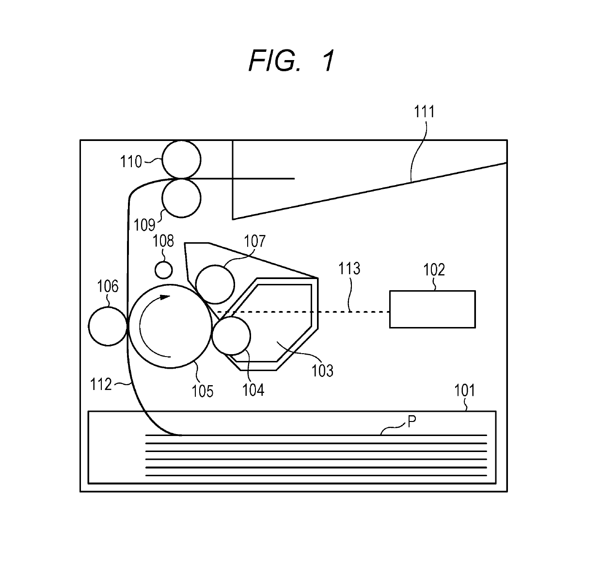
[0021]FIG. 1 is a sectional view for illustrating the schematic structure of a monochrome laser printer being an image forming apparatus to which a pre-exposing device of the first embodiment is applied. In FIG. 1, a sheet feeding unit 101 stores therein sheets P being recording materials, and feeds the sheet P to an image forming unit through a conveyance path112 in printing. The image forming unit configured to form an image on the sheet P fed from the sheet feeding unit 101 includes a laser scanner 102, a toner tank 103, a developing roller 104, a photosensitive drum 105, a transfer roller 106, a charge roller 107, and a light guide 108 of the pre-exposing device. A fixing device configured to fix, onto the sheet P, a toner image transferred onto the sheet P by the image forming unit includes a fixing roller 109 and a pressure roller 110, and the sheet P that has passed through the fixing device ...

second embodiment

[0041]the present invention is described.

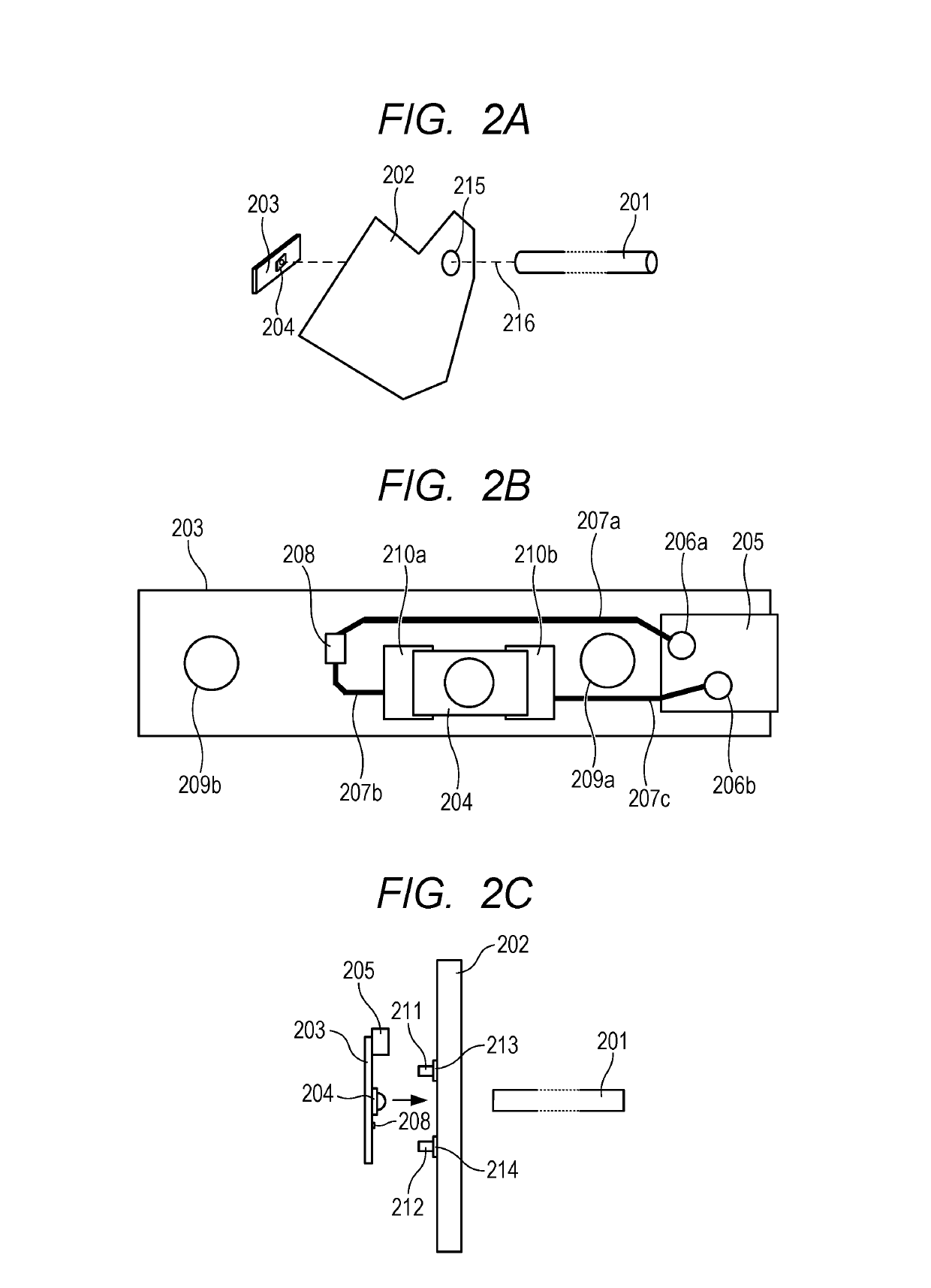
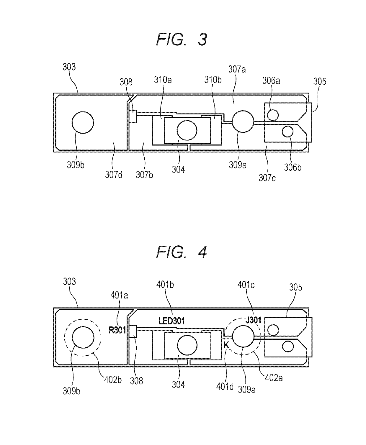
[0042]On circuit boards, symbols for indicating locations (mounting locations) of parts, a mark for indicating the cathode side of a diode, for example, or names, manufacturing numbers, and the like of the circuit boards, which workers can confirm with his / her eyes, are generally drawn by silk screen printing. However, as described above, slight steps on the circuit board leads to the tilt of the circuit board with respect to the mold component. Thus, the silk screen printing, which is performed above the resist layer, is preferably not performed because the silk screen printing may cause difference in height. Further, the silk screen printed portions have great unevenness in thickness unlike the copper foil and the resist, and it is not a good idea to provide the silk screen printed portions in a solid manner like the electro conductive patterns of the first embodiment. Accordingly, in the second embodiment, there is described a method of gi...


PUM


Abstract

The circuit board has a surface mount LED with a lens on the circuit board. A conductive portion and remaining space in the periphery of the LED are covered with solid copper foil so that reflectance of light and a heat dissipation effect are enhanced. In addition, layer structures between the circuit board and an assembled component are the same between contact portions with the assembled component so that tilt in mounting the board is suppressed. As a result, the circuit board having mounted thereon the surface mount LED having high directivity can be accurately mounted on the assembled component, tilt of an optical axis can be suppressed, the reflectance of light from the LED can be increased, and the heat dissipation effect can be enhanced.

Description

BACKGROUND OF THE INVENTIONField of the Invention[0001]The present invention relates to assembly accuracy of a circuit board having mounted thereon a surface mount light emitting element having strong directivity in a predetermined direction.Description of the Related Art[0002]Nowadays, light emitting diodes (hereinafter referred to as “LED”) are popular as compact and inexpensive light sources, and many products use the light emitting diodes not only for indicators but also for illumination and functional parts. The light emitting diodes are used for LED tube lights, backlight of liquid crystal displays, light for illumination of originals on image reading apparatus including scanners, and discharge lamps (hereinafter referred to as “pre-exposing device”) in image forming apparatus, for example. The pre-exposing device is a device configured to lower the surface potential of a photosensitive drum and emit light to the photosensitive drum to achieve uniform potential distribution, a...

Claims


Application Information

Patent Timeline
Patent Type & Authority Patents(United States)
IPC IPC(8): H01L33/00H05K3/00H05K1/18F21K9/238H01L33/48H05K1/02H01L33/60
CPCF21K9/238H01L33/60H01L33/486H05K1/181H05K1/0274H05K3/0064H05K2201/049H05K2201/09063H05K2201/10106
Inventor HIRABAYASHI, JUN
Owner CANON KK
Why Eureka
Try Eureka