Display device and electronic device

a technology of electronic devices and display devices, applied in semiconductor devices, instruments, electrical devices, etc., can solve the problems of reduced yield, difficult miniaturization of transistors, complicated process flow, etc., and achieve the effect of reducing yield, high mask alignment accuracy, and complicated process flow

Active Publication Date: 2019-12-10
SEMICON ENERGY LAB CO LTD
View PDF25 Cites 3 Cited by
  • Summary
  • Abstract
  • Description
  • Claims
  • Application Information

AI Technical Summary

Benefits of technology

[0007]In miniaturization of transistors, high mask alignment accuracy is required in a lithography process. In addition, a margin is required between patterns for a transistor on the assumption of mask misalignment, which makes it difficult to miniaturize transistors. Furthermore, a process flow becomes complicated when the number of lithography processes is large, resulting in a reduction in a yield. Masks are very expensive because they have minute shapes and need to have highly accurate shapes. Moreover, long gate wirings, long source wirings, and the like are used for large display devices; thus, wiring resistance is increased, causing a problem of high power consumption.
[0008]In view of the above, an object of one embodiment of the present invention is to provide a high-definition display device. Another object of one embodiment of the present invention is to provide a display device with high display quality. Another object of one embodiment of the present invention is to provide a display device with low power consumption. Another object of one embodiment of the present invention is to provide a novel display device. Another object of one embodiment of the present invention is to provide a novel electronic device.
[0024]A reduction in the number of lithography processes can reduce a pattern arrangement margin and enables miniaturization of a transistor and an increase in the definition of a display device. Furthermore, a reduction in the number of lithography processes leads to a simple process flow and an improved yield. A reduction in the number of lithography processes can also reduce the cost for masks. When wirings are directly connected to each other in a connection portion, a favorable contact can be obtained and contact resistance can be reduced.
[0025]One embodiment of the present invention can provide a high-definition display device. One embodiment of the present invention can provide a display device with high display quality. One embodiment of the present invention can provide a display device with low power consumption. One embodiment of the present invention can provide a novel display device. One embodiment of the present invention can provide a novel electronic device.

Problems solved by technology

In addition, a margin is required between patterns for a transistor on the assumption of mask misalignment, which makes it difficult to miniaturize transistors.
Furthermore, a process flow becomes complicated when the number of lithography processes is large, resulting in a reduction in a yield.
Masks are very expensive because they have minute shapes and need to have highly accurate shapes.
Moreover, long gate wirings, long source wirings, and the like are used for large display devices; thus, wiring resistance is increased, causing a problem of high power consumption.

Method used


Image

  • Display device and electronic device
  • Display device and electronic device
  • Display device and electronic device

Examples


embodiment 1

[0126]In this embodiment, display devices of one embodiment of the present invention and methods for manufacturing the display devices will be described with reference to FIGS. 1A to 1C to FIGS. 46A to 46D.

example 1

Structure Example 1 of Display Device

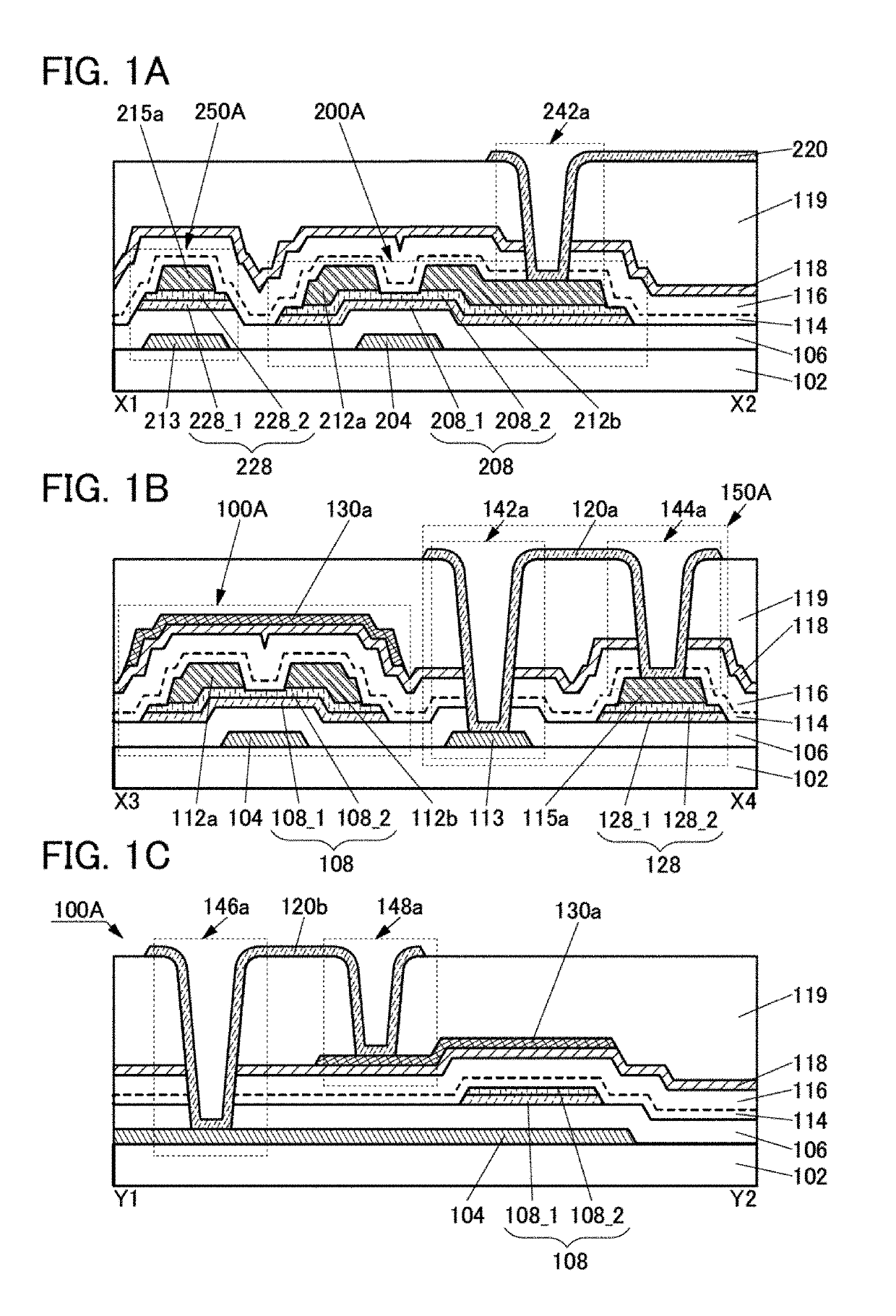
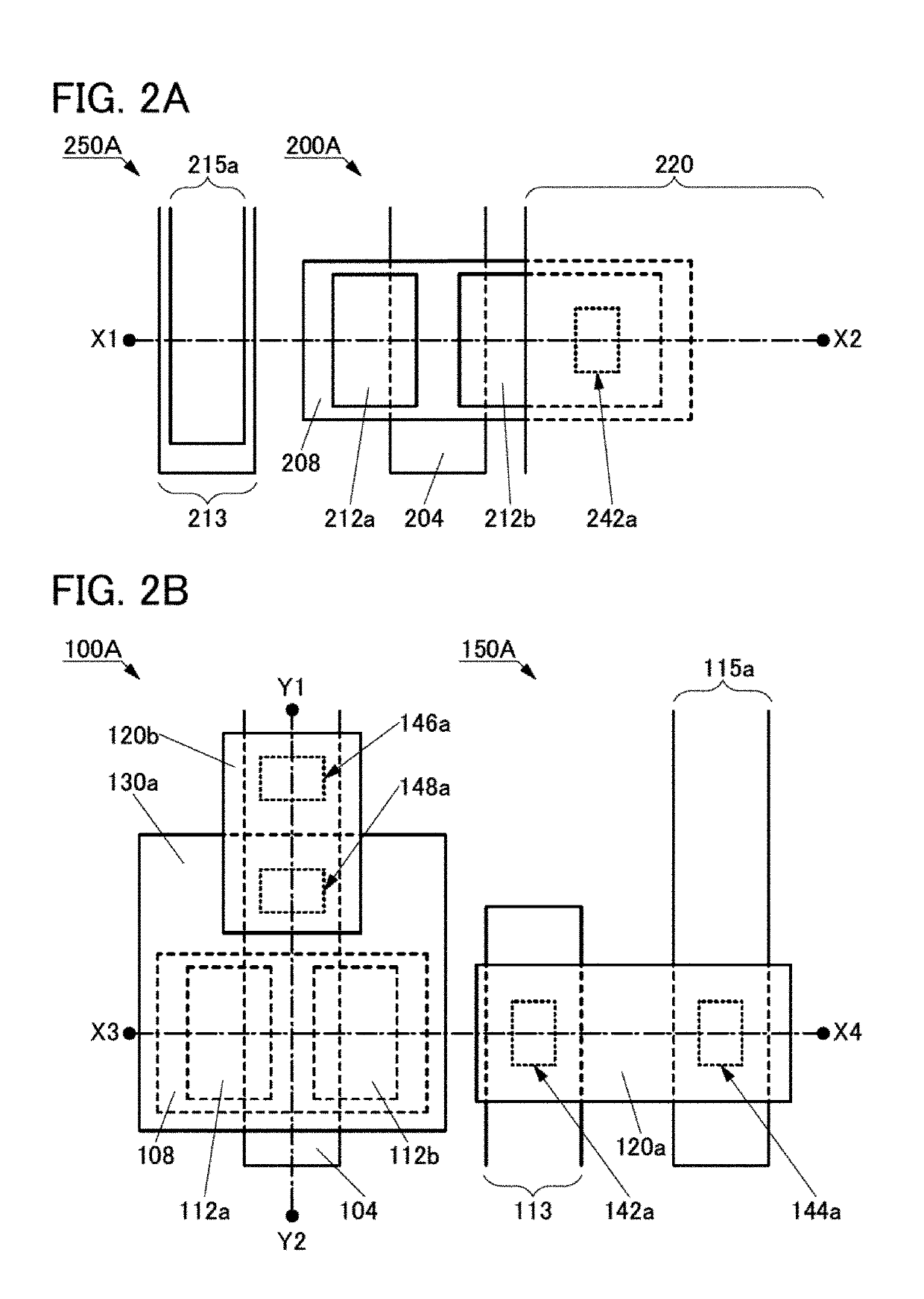
[0127]FIGS. 1A to 1C are cross-sectional views of transistors in a pixel portion and a driver circuit included in a display device of one embodiment of the present invention. FIGS. 2A and 2B are top views of the transistors.

[0128]The display device of one embodiment of the present invention includes a transistor 100A, a transistor 200A, a capacitor 250A, and a connection portion 150A.

[0129]FIG. 1A is a cross-sectional view of the transistor 200A and the capacitor 250A included in the pixel portion, which corresponds to a cross-sectional view taken along dashed-dotted line X1-X2 in FIG. 2A. FIG. 1B is a cross-sectional view of the transistor 100A and the connection portion 150A included in the driver circuit, which corresponds to a cross-sectional view taken along dashed-dotted line X3-X4 in FIG. 2B. FIG. 1C is a cross-sectional view of the transistor 100A included in the driver circuit, which corresponds to a cross-sectional view taken along dash...

example 2

Structure Example 2 of Display Device

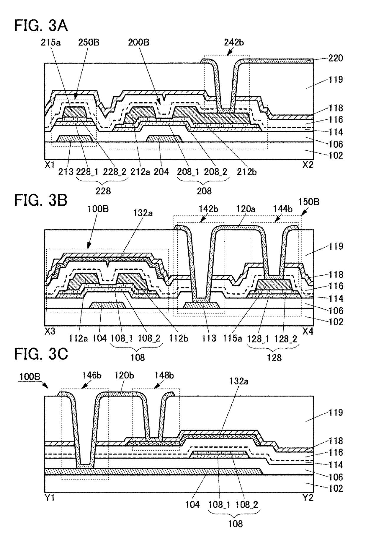
[0232]FIGS. 3A to 3C are cross-sectional views of transistors in a pixel portion and a driver circuit included in another display device of one embodiment of the present invention. The display device illustrated in FIGS. 3A to 3C is different from the display device illustrated in FIGS. 1A to 1C in the transistor structure. Since the top views are similar to those illustrated in FIGS. 2A and 2B, FIGS. 2A and 2B are used for the description.

[0233]The display device of one embodiment of the present invention includes a transistor 100B, a transistor 200B, a capacitor 250B, and a connection portion 150B.

[0234]FIG. 3A is a cross-sectional view of the transistor 200B and the capacitor 250B included in the pixel portion, which corresponds to a cross-sectional view taken along dashed-dotted line X1-X2 in FIG. 2A. FIG. 3B is a cross-sectional view of the transistor 100B and the connection portion 150B included in the driver circuit, which corresponds to a...


PUM


Abstract

The number of lithography processes is reduced and a high-definition display device is provided. The display device includes a pixel portion and a driver circuit for driving the pixel portion. The pixel portion includes a first transistor and a pixel electrode electrically connected to the first transistor. The driver circuit includes a second transistor and a connection portion. The second transistor includes a metal oxide film, first and second gate electrodes that face each other with the metal oxide film positioned therebetween, source and drain electrodes over and in contact with the metal oxide film, and a first wiring connecting the first and second gate electrodes. The connection portion includes a second wiring on the same surface as the first gate electrode, a third wiring on the same surface as the source electrode and the drain electrode, and a fourth wiring connecting the second wiring and the third wiring. The pixel electrode, the first wiring, and the fourth wiring are formed using the same layer.

Description

BACKGROUND OF THE INVENTION1. Field of the Invention[0001]One embodiment of the present invention relates to a display device and an electronic device.[0002]Note that one embodiment of the present invention is not limited to the above technical field. The technical field of one embodiment of the invention disclosed in this specification and the like relates to an object, a method, or a manufacturing method. One embodiment of the present invention relates to a process, a machine, manufacture, or a composition of matter. In particular, one embodiment of the present invention relates to a semiconductor device, a display device, a light-emitting device, a power storage device, a memory device, a driving method thereof, or a manufacturing method thereof.[0003]In this specification and the like, a semiconductor device generally means a device that can function by utilizing semiconductor characteristics. A semiconductor element such as a transistor, a semiconductor circuit, an arithmetic d...

Claims


Application Information

Patent Timeline
Patent Type & Authority Patents(United States)
IPC IPC(8): G09G3/30H01L27/32H01L29/417H01L29/786H01L29/66H01L27/12G09G3/36
CPCG09G3/30H01L27/1288H01L29/78693H01L29/7869H01L29/41733H01L27/1225H01L27/3262H01L29/78696H01L29/66969H01L27/3244H01L27/3276G09G3/3659G09G3/3677H01L2227/323G09G2330/021G09G3/3688H10K59/1213H10K59/131H10K59/1201H10K59/35H10K59/123H10K59/12
Inventor KATAYAMA, MASAHIROKUROSAKI, DAISUKEOKAZAKI, KENICHIKOEZUKA, JUNICHI
Owner SEMICON ENERGY LAB CO LTD
Why Eureka
Try Eureka