Driving substrate, manufacturing process, and micro-LED array light-emitting backlight module

a manufacturing process and backlight module technology, applied in the field of display, can solve the problems of loss of reflectivity, limited reflectivity of traditional coated high-reflective layers (such as white oil), and the inability to perform light recovery, etc., and achieve the effect of enhancing the reflectivity of traditional coated high-reflective layers and reducing the cost of production

Active Publication Date: 2019-12-17
WUHAN CHINA STAR OPTOELECTRONICS TECH CO LTD
View PDF11 Cites 0 Cited by
  • Summary
  • Abstract
  • Description
  • Claims
  • Application Information

AI Technical Summary

Benefits of technology

[0019]In view of the above, the driving substrate, the manufacturing method, and the micro-LED array light emitting backlight module of the present disclosure solve the loss of reflectivity issue caused by the edge forbidden area of the electrode welding pad edge forbidden region. At the same time, the limited reflectivity of traditional coated high-reflective layers (such as white oil) may also be enhanced.

Problems solved by technology

At present, the upper and left / right borders of the display screen are compressed to a very small border to meet the requirements of the full screen at this stage, but at the lower border, due to the need of data line fan-out and reserved chip (IC) bonding areas and flexible circuit board (FPC) bonding areas, further compression of the lower boundary has become a technical problem to be solved.
The spacing between adjacent micro-LEDs 20 is too small, and the occupied area of the micro-LED 20 does not provide effective reflection, and thus light recovery can only be performed through the limited reflection area between the adjacent micro-LEDs 20.
The 99.9% reflectivity of the conventional reflective sheet has certain disadvantages in brightness efficiency.
A certain inhibited area is set around the disc and between adjacent micro-LED positive-negative (PN) electrode pads 21 to prevent the high reflective layer 60 from covering the electrode pads 21 due to process errors, although the inhibited area is single The area is small, but the overall area occupies a large proportion, resulting in the inevitable loss of light efficiency.
Simply increasing the accuracy of etching can hardly overcome the above problems.

Method used


Image

  • Driving substrate, manufacturing process, and micro-LED array light-emitting backlight module
  • Driving substrate, manufacturing process, and micro-LED array light-emitting backlight module
  • Driving substrate, manufacturing process, and micro-LED array light-emitting backlight module

Examples


Embodiment Construction

[0029]The following descriptions for the respective embodiments are specific embodiments capable of being implemented for illustrations of the present invention with referring to appended figures.

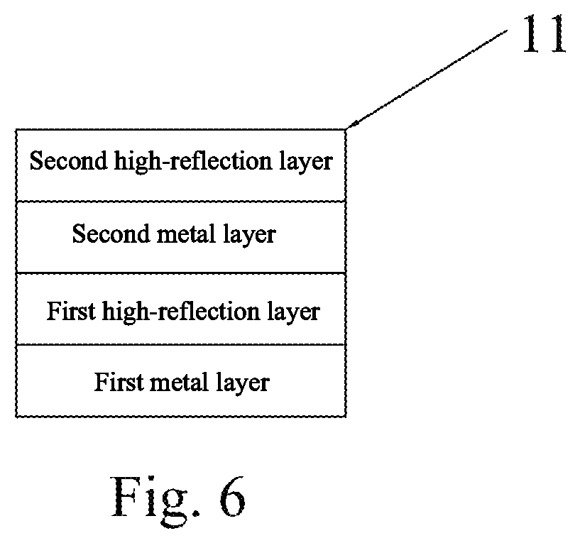
[0030]The driving substrate may be used in micro-LED array light-emitting backlight module. The driving substrate includes: a first metal layer, a first high-reflection layer, and a second metal layer stacked in a top-down sequence. The driving substrate may further includes an insulation supporting layer arranged between the first metal layer and the first high-reflection layer. The driving substrate may include at least a three-layer structure, having the first metal layer, the first high-reflection layer, and a second metal layer. Alternatively, the driving substrate may include at least a four-layer structure, having the first metal layer, the insulation supporting layer, the first high-reflection layer, and the second metal layer.

[0031]In one embodiment, the driving substrate may furth...


PUM

PropertyMeasurementUnit
sizeaaaaaaaaaa
reflectanceaaaaaaaaaa
reflectivityaaaaaaaaaa

Abstract

The present disclosure relates to a driving substrate, a manufacturing method, and a micro-LED array substrate light-emitting backlight module. The driving substrate includes a first metal layer, a first high-reflection layer, and a second metal layer stacked in a top-down sequence. The driving substrate, the manufacturing method, and the micro-LED array light emitting backlight module of the present disclosure solve the loss of reflectivity issue caused by the edge forbidden area of the electrode welding pad edge forbidden region. At the same time, the limited reflectivity of traditional coated high-reflective layers (such as white oil) may also be enhanced.

Description

FIELD OF THE INVENTION[0001]The present disclosure relates to a display field, and more particularly to a driving substrate, a manufacturing process, and a micro-LED array light-emitting backlight module.BACKGROUND OF THE INVENTION[0002]With the gradual emergence of wearable application devices, such as smart glasses, smart watches, etc., the display industry's demand for flexible display devices has been increased. Organic Light Emitting Display (OLED) has the attributes of self-illumination, no need of backlight, thin thickness, wide viewing angle, fast response, and so on. Such attributes bring in the advantages for flexible displays. With the competition of flexible OLEDs, traditional liquid crystal display technology has gradually adopted flexible substrates to make breakthroughs in the direction of flexibility and curved surfaces. It can be seen that the era of flexible and curved display is approaching.[0003]FIG. 1 shows a schematic diagram of a border design of a conventiona...

Claims


Application Information

Patent Timeline
Patent Type & Authority Patents(United States)
IPC IPC(8): H05K1/02G02F1/1335H05K3/04
CPCH05K1/028G02F1/133606G02F1/133603G02F1/133605H05K3/04H05K2201/0154G02F2001/133612H05K2201/10106G02F2001/133614H05K1/189H05K1/0274H05K2201/2054H05K1/09H05K2201/0338G02F1/133612G02F1/133614
Inventor ZHA, GUOWEI
Owner WUHAN CHINA STAR OPTOELECTRONICS TECH CO LTD
Why Eureka
Try Eureka