Light emitting diode having a current blocking layer

a technology of light emitting diodes and current blocking layers, which is applied in the direction of basic electric elements, semiconductor devices, electrical equipment, etc., can solve the problems of difficult heat radiating to the outside, increased heat loss rate, and thermal degradation phenomenon, so as to improve reliability, prevent thermal degradation phenomenon, and prolong life

Active Publication Date: 2020-01-21
SUZHOU LEKIN SEMICON CO LTD
View PDF19 Cites 0 Cited by
  • Summary
  • Abstract
  • Description
  • Claims
  • Application Information

AI Technical Summary

Benefits of technology

[0024]A light emitting device and a light emitting device package including the same according to embodiments have improved reliability in which a thermal degradation phenomenon can be prevented by a current blocking layer disposed in an ohmic layer, a prolonged lifetime can be achieved by improving a heat loss rate even at a high driving voltage, and the like.

Problems solved by technology

In the case of the above-described light emitting device and a light emitting device package including the same, since a path through which carriers are supplied and a path through which heat is radiated are the same, a thermal degradation phenomenon, in which it is difficult for heat to radiate to the outside, may occur.
Particularly, in a case in which the light emitting device emits deep ultraviolet light, a heat loss rate may be further increased due to a high driving voltage.

Method used


Image

  • Light emitting diode having a current blocking layer
  • Light emitting diode having a current blocking layer
  • Light emitting diode having a current blocking layer

Examples


first embodiment

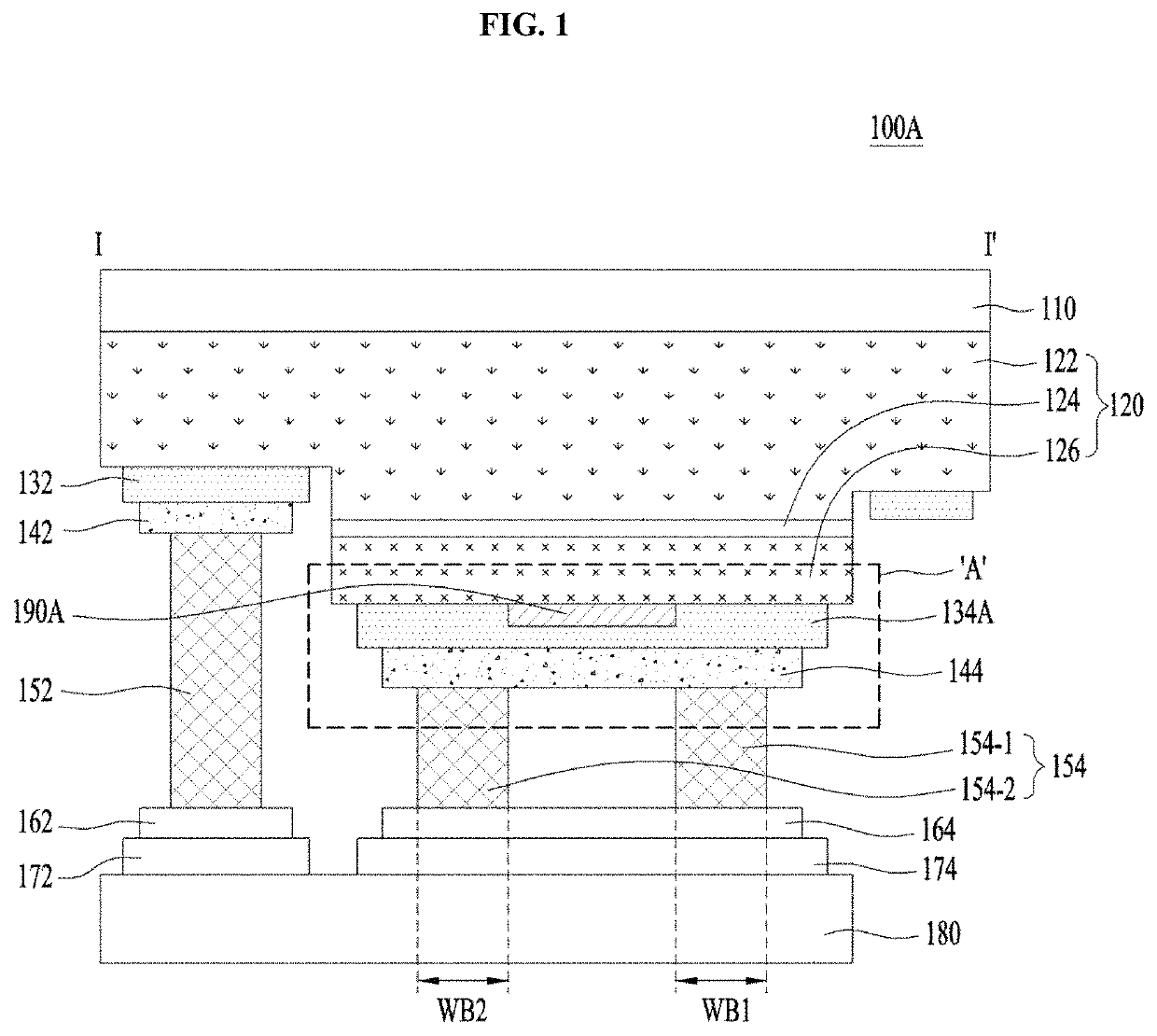
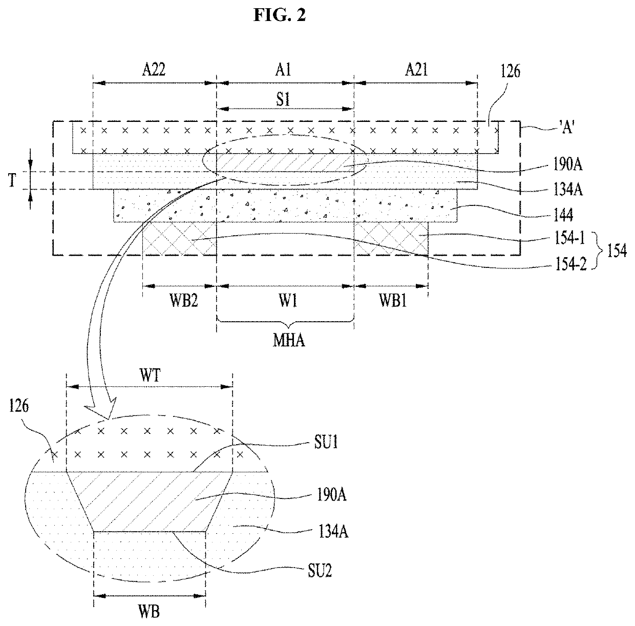
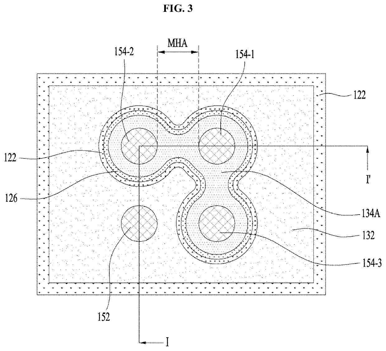
[0039]FIG. 1 is a cross-sectional view illustrating a light emitting device 100A FIG. 2 is an enlarged cross-sectional view illustrating a portion ‘A’ illustrated in FIG. 1, and FIG. 3 is a bottom view illustrating an example of the light emitting device 100A illustrated in FIG. 1.

[0040]Although FIG. 1 corresponds to a cross-sectional view taken along line I-I′ illustrated in FIG. 3, the embodiment is not limited thereto. That is, the light emitting device 100A illustrated in FIG. 1 may also have various bottom views other than the bottom view illustrated in FIG. 3.

[0041]The light emitting device 100A illustrated in FIG. 1 may include a substrate 110, a light emitting structure 120, first and second ohmic layers (or contact layers or electrodes) 132 and 134A, first and second spreading layers 142 and 144, at least one first bump 152, a plurality of second bumps 154, first and second metal pads 162 and 164, first and second insulating layers 172 and 174, a submount 180, and a curren...

second embodiment

[0083]FIG. 4 is a cross-sectional view illustrating a light emitting device 100B and FIG. 5 is an enlarged cross-sectional view illustrating a portion ‘B’ illustrated in FIG. 4.

[0084]Like the light emitting device 100A illustrated in FIG. 1, a light emitting device 100B illustrated in FIG. 4 corresponds to a cross-sectional view taken along line I-I′ illustrated in FIG. 3, but the embodiment is not limited thereto. That is, the light emitting device 100B illustrated in FIG. 4 may also have various bottom views other than the bottom view illustrated in FIG. 3.

[0085]The light emitting device 100B illustrated in FIG. 4 may include a substrate 110, a light emitting structure 120, first and second ohmic layers 132 and 134B, first and second spreading layers 142 and 144, a first bump 152, a plurality of second bumps 154, first and second metal pads 162 and 164, first and second insulating layers 172 and 174, a submount 180, and a current blocking layer 190B.

[0086]Here, since the substrat...

third embodiment

[0099]FIG. 6 is a cross-sectional view illustrating a light emitting device 100C according to a

[0100]Like the light emitting device 100A illustrated in FIG. 1, a light emitting device 100C illustrated in FIG. 6 corresponds to a cross-sectional view taken along line I-I′ illustrated in FIG. 3, but the embodiment is not limited thereto. That is, the light emitting device 100C illustrated in FIG. 6 may also have various bottom views other than the bottom view illustrated in FIG. 3.

[0101]The light emitting device 100C illustrated in FIG. 6 may include a substrate 110, a light emitting structure 120, first and second ohmic layers 132 and 134C, first and second spreading layers 142 and 144, a first bump 152, a plurality of second bumps 154, first and second metal pads 162 and 164, first and second insulating layers 172 and 174, a submount 180, and a current blocking layer 190C.

[0102]Since the substrate 110, the light emitting structure 120, the first ohmic layer 132, the first and second ...


PUM

PropertyMeasurementUnit
widthaaaaaaaaaa
distanceaaaaaaaaaa
distanceaaaaaaaaaa

Abstract

A light emitting device according to embodiments includes a substrate, a light emitting structure disposed under the substrate and including a first conductive semiconductor layer, an active layer, and a second conductive semiconductor layer, a submount disposed to face the substrate, first and second metal pads disposed on the submount to be spaced apart from each other, a first bump disposed on the first metal pad, a plurality of second bumps disposed on the second metal pad to be spaced apart from each other, a first ohmic layer interposed between the first conductive semiconductor layer and the first bump, a second ohmic layer interposed between the second conductive semiconductor layer and the plurality of second bumps, a first spreading layer interposed between the first ohmic layer and the first bump, a second spreading layer interposed between the second ohmic layer and the plurality of second bumps, and a current blocking layer disposed in a maximum heating area of the second ohmic layer overlapping an area between the plurality of second bumps in a thickness direction of the light emitting structure such that the current blocking layer does not cut the second ohmic layer in a horizontal direction intersecting the thickness direction.

Description

CROSS-REFERENCE TO RELATED PATENT APPLICATIONS[0001]This application is a U.S. National Stage Application under 35 U.S.C. § 371 of PCT Application No. PCT / KR2017 / 000179, filed Jan. 6, 2017, which claims priority to Korean Patent Application No. 10-2016-0001833, filed Jan. 7, 2016, whose entire disclosures are hereby incorporated by reference.TECHNICAL FIELD[0002]The present invention relates to a light emitting device.BACKGROUND ART[0003]A light emitting diode (LED) is a kind of semiconductor that converts electricity into infrared light or light used for receiving or transmitting signals or used as a light source by utilizing properties of a compound semiconductor.[0004]Group III-V nitride semiconductors have been in the spotlight as important materials of light emitting devices such as an LED or laser diode (LD) due to physical and chemical properties thereof.[0005]Since LEDs do not contain environmentally hazardous substances such as mercury (Hg), which is used in conventional li...

Claims


Application Information

Patent Timeline
Patent Type & Authority Patents(United States)
IPC IPC(8): H01L33/14H01L33/32H01L33/62H01L33/36
CPCH01L33/62H01L33/145H01L33/36H01L33/32H01L33/38H01L2224/48091H01L2224/14H01L33/44H01L33/486H01L2924/00014
Inventor SONG, HYUN DON
Owner SUZHOU LEKIN SEMICON CO LTD
Why Eureka
Try Eureka