

Method of identifying defect regions in wafer
a defect region and silicon wafer technology, applied in semiconductor/solid-state device testing/measurement, instruments, material analysis, etc., can solve problems such as residual oi, reduced wafer strength, and differences in gettering ability
- Summary
- Abstract
- Description
- Claims
- Application Information
AI Technical Summary
Benefits of technology
Problems solved by technology
Method used
Image

Examples
Embodiment Construction
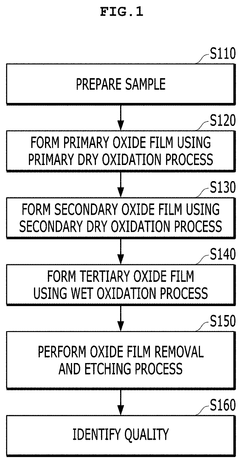
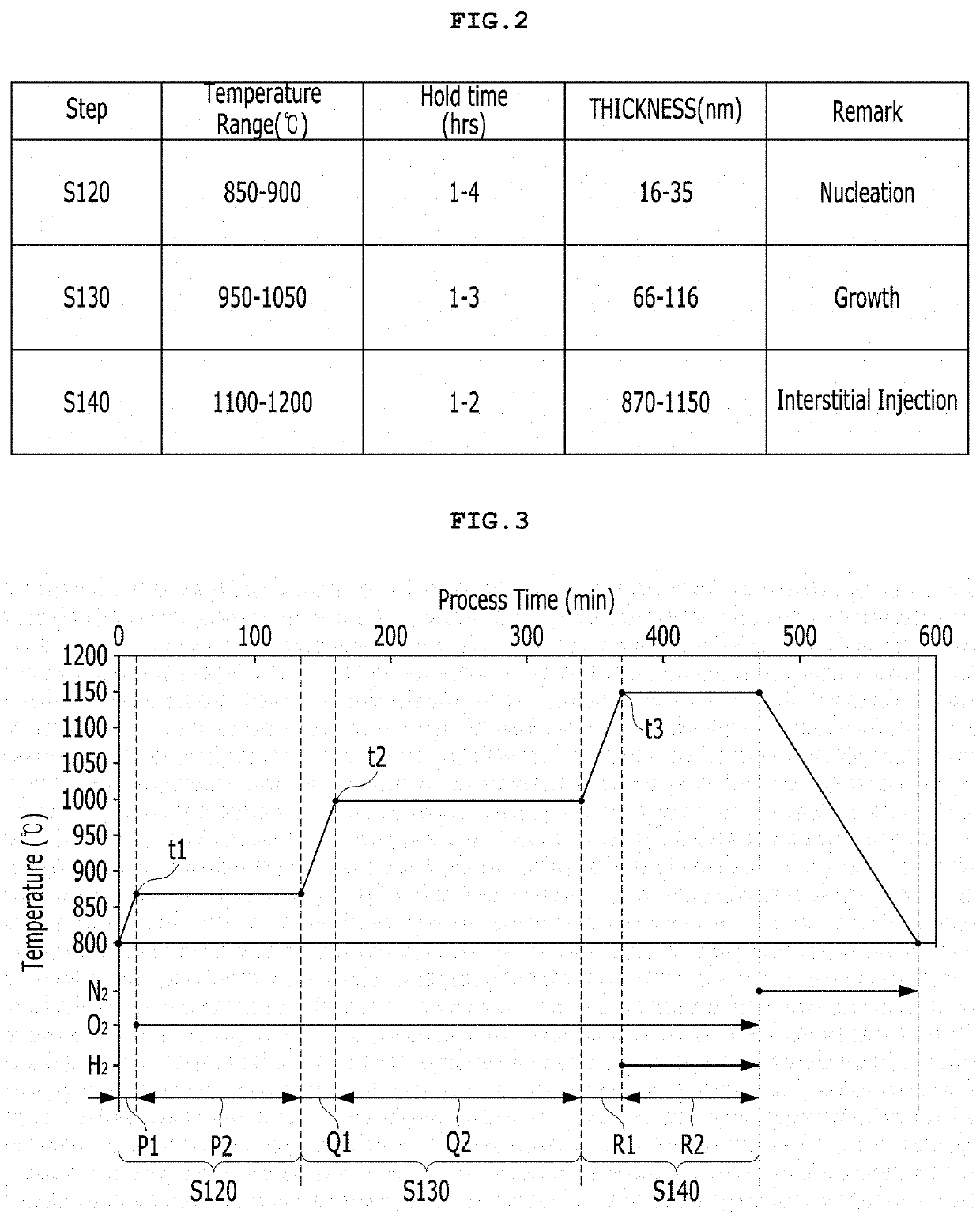
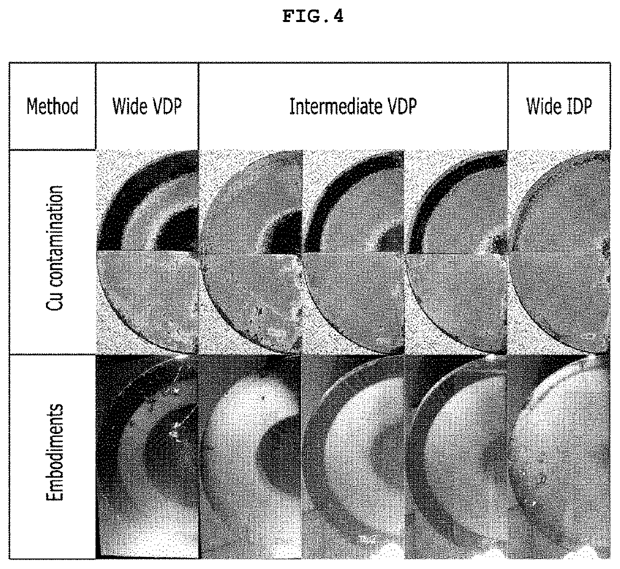
[0034]Reference will now be made in detail to the preferred embodiments of the embodiments, examples of which are illustrated in the accompanying drawings.
[0035]In description of exemplary embodiments, it will be understood that, when an element is referred to as being “on” or “under” another element, the element can be directly on another element or intervening elements may be present. In addition, when an element is referred to as being “on” or “under” another element, this may include the meaning of an upward direction or a downward direction based on one component.
[0036]In addition, in the description of the various embodiments, although relative terms such as, for example, “first”, “second”, “on / upper / above” and “beneath / lower / below may be used to distinguish any one substance or element with another substance or element without requiring or containing any physical or logical relationship or sequence between these substances or elements. Wherever possible, the same reference nu...
PUM
| Property | Measurement | Unit |
|---|---|---|
| temperature | aaaaa | aaaaa |
| temperature | aaaaa | aaaaa |
| temperature | aaaaa | aaaaa |
Abstract
Description
Claims
Application Information