
Optical multiplexing circuit

a multiplexing circuit and optical technology, applied in the field of optical multiplexing circuits, can solve the problems of difficult to multiplex light beams with three or more wavelengths by using mmi, and achieve the effects of reducing the coupling length

Active Publication Date: 2020-05-12
NIPPON TELEGRAPH & TELEPHONE CORP
View PDF26 Cites 4 Cited by
  • Summary
  • Abstract
  • Description
  • Claims
  • Application Information

AI Technical Summary

Benefits of technology

[0020]According to the present invention, even in the case of multiplexing a plurality of light beams with a plurality of wavelengths using a PLC, if conditions for coupling the light beams with desired wavelengths are satisfied, it is possible to suppress coupling of the light beams with the other wavelengths and couple and multiplex only the light beams with the desired wavelengths. Then, the gap at each directional coupler can be narrowed within the fabrication capability, and accordingly the coupling length can be shortened. It is therefore possible to make an efficient and small optical multiplexing circuit.
[0021]Moreover, according to the present invention, the intensity of existing light from an RGB multiplexing circuit using a planar lightwave circuit by be raised by using a space multiplexing technique.

Problems solved by technology

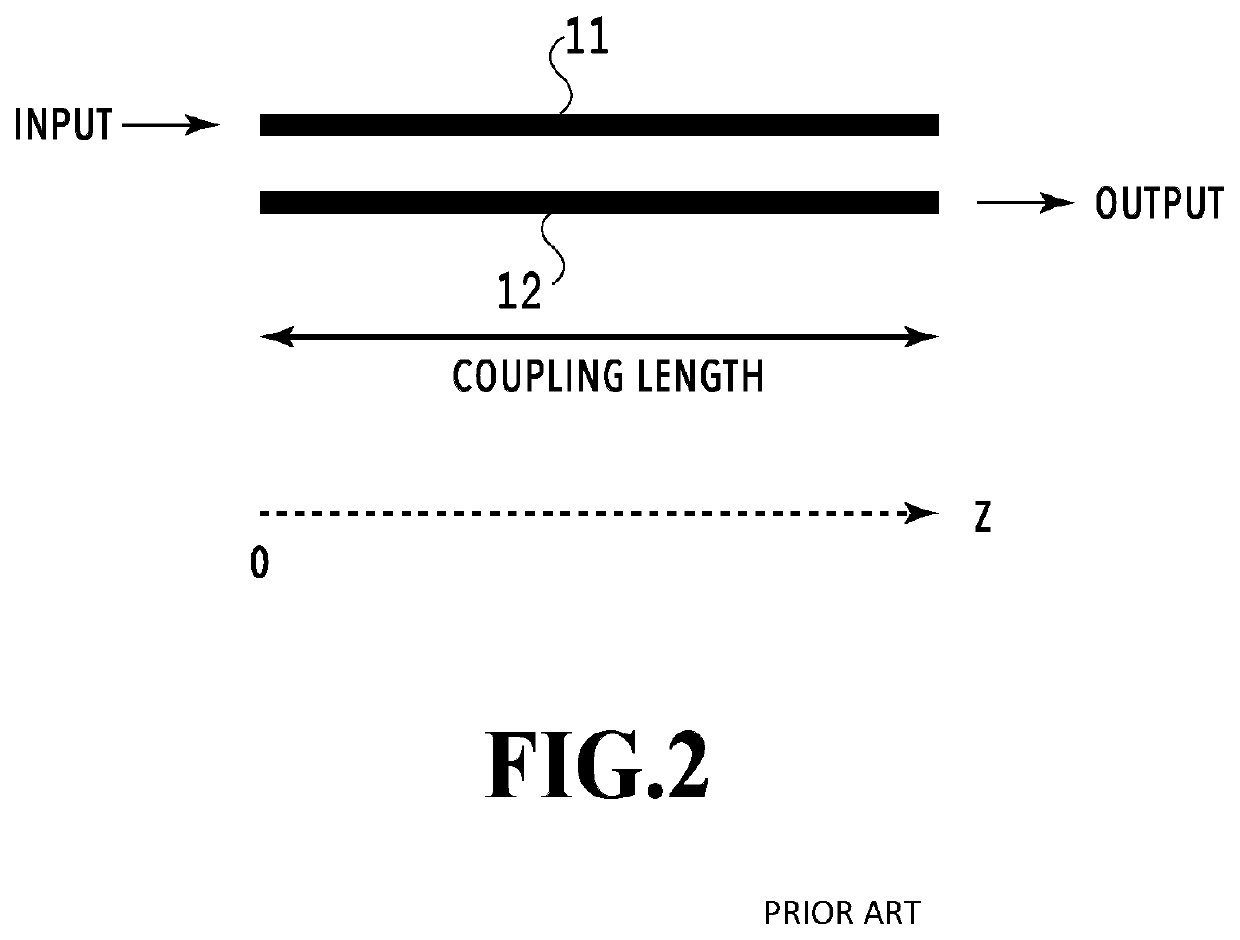
However, since each of the number of input waveguides and the number of output waveguides is two, it is difficult to multiplex light beams with three or more wavelengths by using MMI.

Method used


Image

  • Optical multiplexing circuit
  • Optical multiplexing circuit
  • Optical multiplexing circuit

Examples


embodiment 1

[0033]An optical multiplexing circuit according to embodiment 1 of the present invention will be specifically described with reference to FIGS. 4 to 6. In this embodiment, light beams with wavelengths λ1, λ2, and λ3 are light beams with wavelengths in blue (400 to 495 nm), green (495 to 570 nm), and red (620 to 750 nm) wavelength bands, respectively.

[0034]FIG. 4 exemplarily illustrates the optical multiplexing circuit according to embodiment 1 of the present invention. FIG. 4 illustrates an optical multiplexing circuit including a first optical waveguide 101 in which the light beam with the wavelength λ3 is input, a second optical waveguide 102 in which the light beams with the wavelengths λ1 and λ2 are input, a multi-mode (MM) conversion waveguide 103, a first coupling part 104, a second coupling part 105, and an output waveguide 106 coupled to the second optical waveguide 102. Here, in this embodiment 1, description will be given of an example where the two light beams with the wa...

embodiment 2

[0047]An optical multiplexing circuit according to embodiment 2 of the present invention will be specifically described with reference to FIGS. 8 to 10. FIG. 8 is a diagram exemplarily illustrating the optical multiplexing circuit according to the embodiment of the present invention. FIG. 8 illustrates an optical multiplexing circuit including first to third waveguides 201 to 203, a multiplexing optical waveguide 204, first to third multiplexing parts 205 to 207, and an output waveguide 208 coupled to the multiplexing optical waveguide 204.

[0048]The first to third optical waveguide 201 to 203 and the multiplexing optical waveguide 204 are formed of a lower cladding layer provided on a substrate, a core layer higher in refractive index than the lower cladding layer, and an upper cladding layer provided on the core layer. The upper cladding layer is provided so as to surround the core layer. The first to third optical waveguides 201 to 203 can be single-mode waveguides. The multiplexi...

embodiment 3

[0065]An optical multiplexing circuit according to embodiment 3 of the present invention will be specifically described with reference to FIG. 11. In this embodiment 3, an optical multiplexing circuit will be discussed which has a function of coupling and multiplexing only light beams with desired wavelengths as in embodiment 1 and a function of multiplexing light beams with wavelengths in different waveguide modes to thereby output a multiplexed light beam with higher intensity as in embodiment 2.

[0066]FIG. 11 illustrates an optical multiplexing circuit including first to fifth optical waveguides 301 to 305 into which light beams with wavelengths λ1, λ2, λ3, λ2′ and λ3′ are input, respectively, first and second MM conversion waveguides 306 and 307, first to fourth coupling parts 308 to 311, first and second multiplexing parts 312 and 313, and an output waveguide 314 coupled to the first optical waveguide 301.

[0067]The first to fifth optical waveguides 301 to 305 and the first and s...


PUM

PropertyMeasurementUnit
refractive indexaaaaaaaaaa
wavelength bandsaaaaaaaaaa

Abstract

Provided is an optical multiplexing circuit. The waveguide width of each waveguide is set such that the effective refractive index of a first optical waveguide with a first light beam in the 0-th order mode is equal to the effective refractive index of a MM conversion waveguide with the first light beam in the higher order mode and that the effective refractive indexes of the MM conversion waveguide with second and third light beams in the higher order mode are not equal to the effective refractive indexes of a second optical waveguide with the second and third light beams in the 0-th order mode.

Description

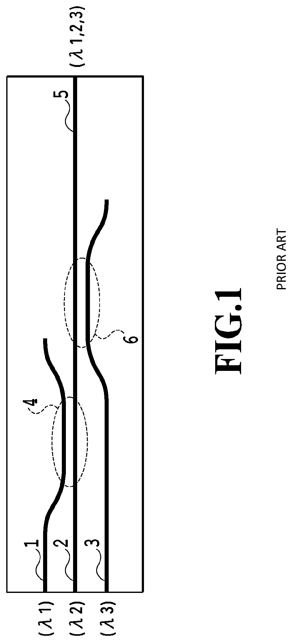
TECHNICAL FIELD[0001]The present invention relates to an optical multiplexing circuit and more specifically relates to, for example, a three-primary-color optical multiplexing circuit that multiplexes visible light beams having three primary colors, namely, R, G, and B light beams (R: red light, G: green light, B: blue light).BACKGROUND ART[0002]In recent years, an RGB coupler module using a silica-based planar lightwave circuit (PLC) has been drawing attention as a circuit element that multiplexes visible light beams of three primary colors for eyeglass-type devices and projectors (see Non Patent Literature 1, for example). In the PLC, optical waveguides are created in a planar substrate by patterning and etching processes in photolithography or the like and a plurality of basic optical circuits (e.g. directional couplers, Mach-Zehnder interferometers, etc.) are combined with each other to implement various functions.[0003]There is a three-primary-color multiplexing circuit that ut...

Claims


Application Information

Patent Timeline
Patent Type & Authority Patents(United States)
IPC IPC(8): G02B6/293G02B6/12G02B6/14
CPCG02B6/29344G02B6/12007G02B6/2938G02B6/14G02B6/29332
Inventor SAKAMOTO, JUNJIWATANABE, KEIHASHIMOTO, TOSHIKAZU
Owner NIPPON TELEGRAPH & TELEPHONE CORP
Learn More