Power drop reset circuit for power supply chip and power drop reset signal generating method

Active Publication Date: 2020-05-26
WINBOND ELECTRONICS CORP
View PDF6 Cites 0 Cited by
  • Summary
  • Abstract
  • Description
  • Claims
  • Application Information

AI Technical Summary

Benefits of technology

The patent text describes a power drop reset circuit and a method for generating a power drop reset. The aim is to solve the problems that arise due to power drops in electronic devices. The technical effect of this patent is to provide a solution for power drop resets that improves the reliability and efficiency of electronic devices.

Problems solved by technology

Since characteristics of a realistic power supply chip may not match the characteristics of an ideal power supply chip, the POR mechanism might not function as intended.
However, a realistic POR circuit might not match such characteristics.
Also, the Vcc might not drop low enough in order for the POR circuit to be set for a POR.
First, it is not easy to have the Vcc operating voltage exactly meeting the intended voltage in order for the POR to occur.
Second, the Vcc operating voltage might not drop far enough below the lowest Vcc operating voltage level.
Third, it is not easy to design the POR circuit because the POR circuit should consume just about no current when the power supply chip is at a standby mode.

Method used


Image

  • Power drop reset circuit for power supply chip and power drop reset signal generating method
  • Power drop reset circuit for power supply chip and power drop reset signal generating method
  • Power drop reset circuit for power supply chip and power drop reset signal generating method

Examples


Embodiment Construction

[0022]Reference will now be made in detail to the present exemplary embodiments of the disclosure, examples of which are illustrated in the accompanying drawings. Wherever possible, the same reference numbers are used in the drawings and the description to refer to the same or like parts.

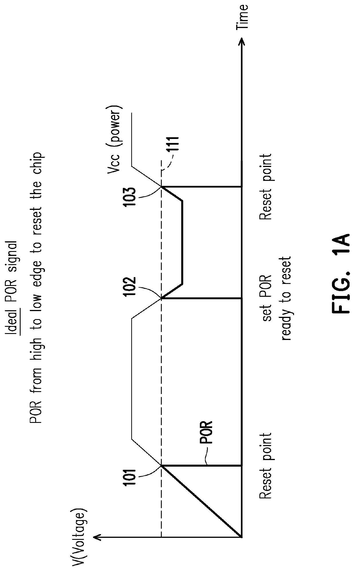
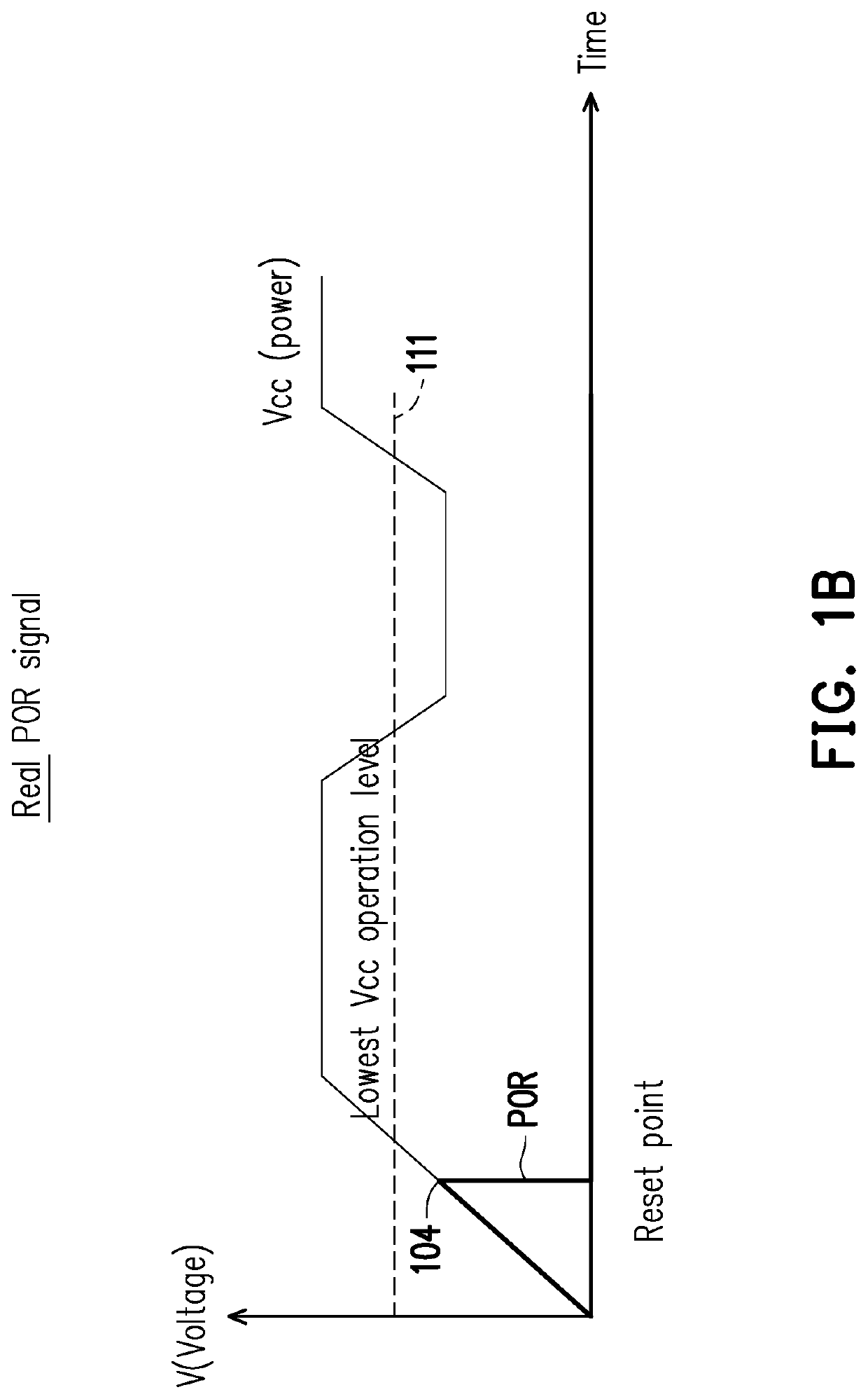
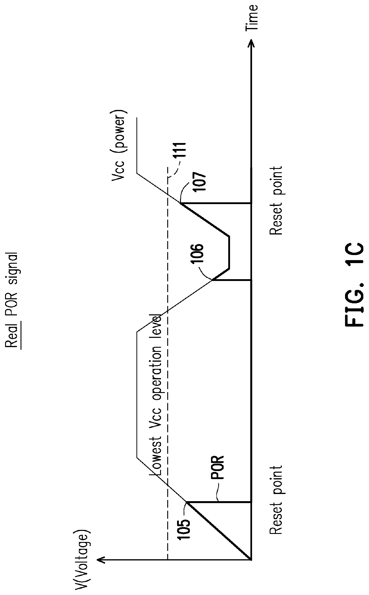
[0023]In order to address some or all of the above described problems, the disclosure provides a power drop reset circuit used by a POR circuit of a power supply chip and a power drop reset signal generating method. FIG. 2 illustrates a functional block diagram of a power drop reset circuit with power drop detection mechanism in accordance with one of the exemplary embodiments of the disclosure. The power drop reset circuit would include not limited to a first step circuit 201 and a second step circuit 202 which is connected to the first step circuit. The power drop reset circuit could be a part of a POR circuit of a power supply chip and would generate a reset signal to reset the power supply chip ...


PUM


Abstract

The disclosure is directed to a power drop reset circuit which includes not limited to: a first step circuit configured to detect a change of a power supply voltage per unit of time and transmit an enable signal in response to the first step circuit having determined that the change of the power supply voltage per unit of time has dropped below zero, wherein the first step circuit does not consume any current when the Vcc change per unit of time is greater than or equal to zero; and a second step circuit electrically connected to the first step circuit and configured to detect the Vcc in response to having received the enable signal and generate a power drop reset signal in response to having determined that the Vcc has dropped below a predetermined operating voltage, wherein the second step circuit consumes an operating current after receiving the enable signal.

Description

TECHNICAL FIELD[0001]The present disclosure is directed to a power drop reset circuit used by a power supply chip and a power drop reset signal generating method.BACKGROUND[0002]Conventionally, a power on reset (POR) circuit is used to generate a power on reset signal for a power supply chip and to trigger a power up read signal which is for reading status bits in order to obtain the current status information of the power supply chip. A system wide reboot could be triggered after the bias voltage (Vcc) of the power supply chip drops to an operating voltage that is below a predetermined Vcc operating voltage but above the ground voltage. The POR circuit is used by a power supply chip which normally is not allowed to consume current while the power supply chip is in a standby mode, but a power drop may nevertheless occur while the power supply chip is in the standby mode. Since characteristics of a realistic power supply chip may not match the characteristics of an ideal power supply...

Claims


Application Information

Patent Timeline
IPC IPC(8): H03K3/02H03K3/012H03K5/02H03K19/21
CPCH03K3/012H03K5/02H03K19/21H03K17/22H03K17/223
Inventor HUANG, KOYING
Owner WINBOND ELECTRONICS CORP
Why Eureka
Try Eureka