Level shifter

a level shifter and level technology, applied in the field of level shifters, can solve the problems of inhibiting normal operation, draining current, and inability to achieve high-speed operation, and achieve the effect of high resistance and faster level shift operation

Inactive Publication Date: 2006-09-21
SOCIONEXT INC
View PDF5 Cites 39 Cited by
  • Summary
  • Abstract
  • Description
  • Claims
  • Application Information

AI Technical Summary

Benefits of technology

[0054] According to the present invention, during a predetermined time period after the connection of the gate of the first or second second-conductivity type transistor is switched from the ground to the second voltage supply, the potential at the gate of the first or second second-conductivity t

Problems solved by technology

However, in the above-described conventional level shifter, if the ON resistance value of the P-type transistors P51 and P52 is increased to achieve a low-voltage operation, the drain currents of the P-type transistors P51 and P52 become small at the time of increasing the potentials of the nodes W51 and W52, and as a result, a high-speed operation cannot be achieved.
If this potential decrease level becomes greater than the threshold voltage of the P-type transistor P51 or P52, the P-type transistor P51 or P52 cannot be turned OFF, so that the level shifter can cause a malfunction.
Furthermore, in the N-type transistors N51 and N52 for signal input, the OFF leakage current increases even when the threshold voltage is decreased due to a variation in temperature or production process thereof, thereby inhibiting the normal operation.
If this potential decrease level becomes greater than the threshold voltage of the P-type transistor P51 or P52, the P-type transistor P51 or P52 cannot be turned OFF, so that the level shifter can cause a malfunction.
Furthermore, in the N-type

Method used


Image

  • Level shifter
  • Level shifter
  • Level shifter

Examples


embodiment 1

[0084] (Embodiment 1)

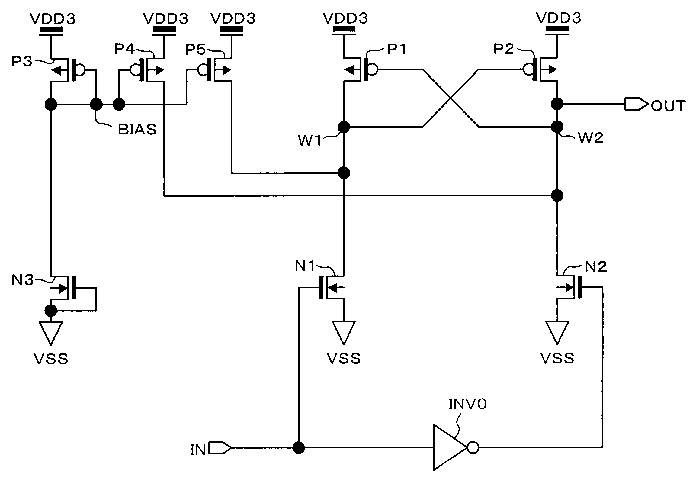
[0085]FIG. 1 shows a specific structure of a level shifter according to embodiment 1.

[0086] In FIG. 1, a terminal IN is a signal input terminal, an element INV0 is an inverter formed by a lower voltage side element for inverting a signal input through the input terminal IN. The inverter INV0 operates with lower voltage supply (first voltage supply) VDD of, for example, 1.5 V.

[0087] In FIG. 1, the elements other than the inverter INV0 are elements on the higher voltage side at, for example, 3.3 V. The level shifter includes a pair of N-type transistors N1 and N2 for complementary signal input, which has sources connected to the ground. The gate of the N-type transistor N1 (first first-conductivity type transistor) receives a signal input through the input terminal IN (one of complementary first and second input signals). The gate of the N-type transistor N2 (second first-conductivity type transistor) receives an output signal of the inverter INV0 (the other of ...

embodiment 2

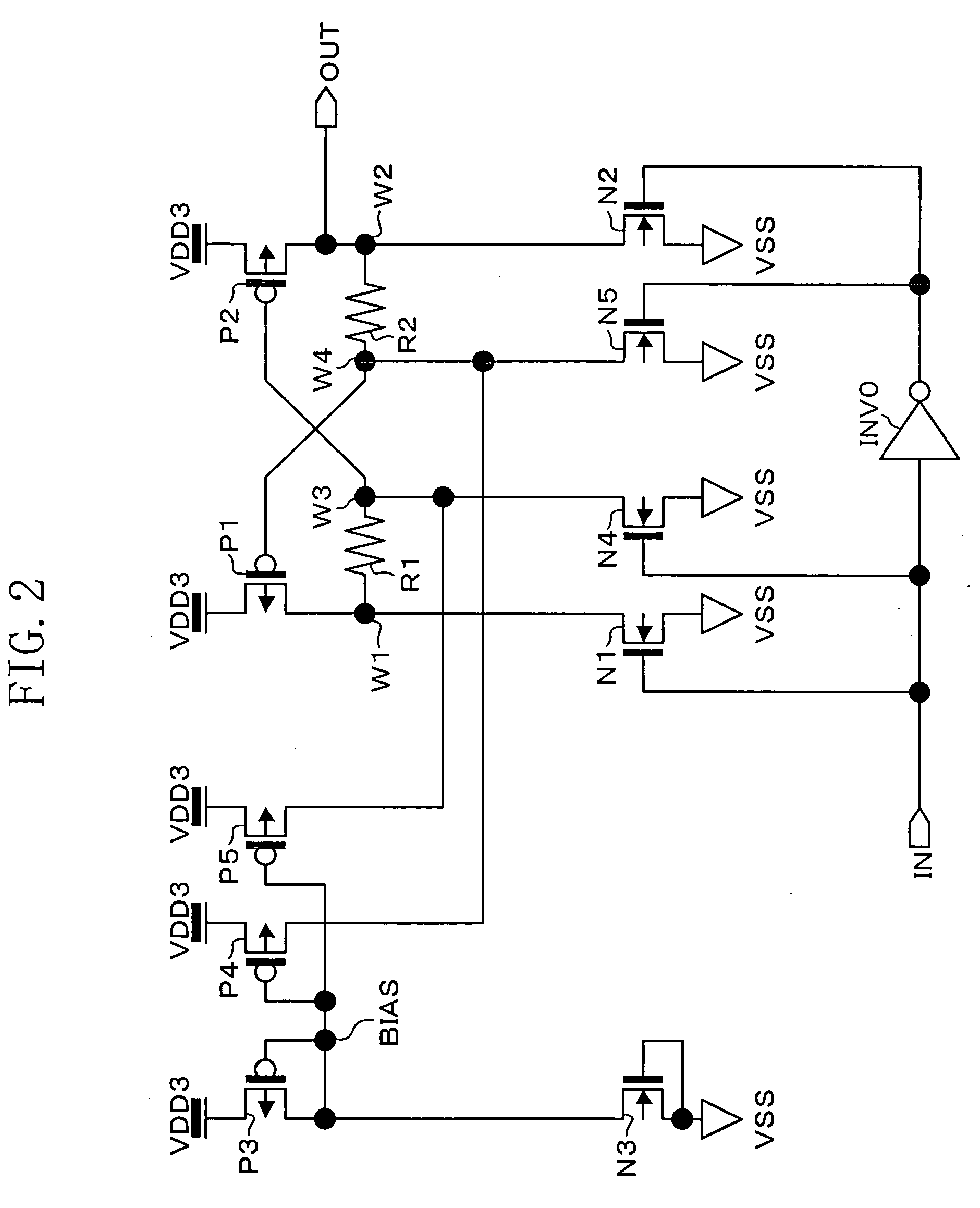
[0119] (Embodiment 2)

[0120]FIG. 5 shows a specific structure of a level shifter of embodiment 2.

[0121] The level shifter of FIG. 5 includes, in addition to the components of the level shifter of FIG. 1 of embodiment 1, a P-type transistor P8 which is provided in place of the P-type transistors P4 and P5. The source of the P-type transistor P8 is connected to higher voltage supply VDD3. The gate of the P-type transistor P8 is connected to the node BIAS. The P-type transistor P8 cooperates with the P-type transistor P3 as a current mirror and forms a current conversion circuit which amplifies the OFF leakage current flowing through the N-type transistor N3 by a predetermined factor to generate a current flowing from higher voltage supply VDD3. The level shifter of FIG. 5 further includes P-type transistors P9 and P10 which constitute a switch circuit for connecting the drain of the P-type transistor P8 to any one of the nodes W1 and W2. The sources of the P-type transistors P9 and P1...

embodiment 3

[0127] (Embodiment 3)

[0128]FIG. 6 shows a specific structure of a level shifter of embodiment 3.

[0129] The level shifter of FIG. 6 is different from the level shifter of FIG. 5 of embodiment 2 in that the P-type transistor P10 is merged into the P-type transistor P1 and the P-type transistor P9 is merged into the P-type transistor P2. The drain of the P-type transistor P8 is connected to the sources of the P-type transistors P1 and P2. The P-type transistors P9 and P10 of FIG. 5 are not shown because they are merged into the P-type transistors P2 and P1, respectively. The other part of the structure is the same as that of embodiment 2.

[0130] The operation of the level shifter of embodiment 3 is the same as that of the level shifter of FIG. 5 of embodiment 2. The level shifter of embodiment 3 is formed by a smaller number of transistors than the level shifter of embodiment 2, and therefore, the same operation of the level shifter is realized with a smaller circuit area as compared ...


PUM


Abstract

In a level shifter, OFF leakage currents flow through two N-type transistors for signal input even when they are OFF. However, another N-type transistor serving as an OFF leakage generation circuit and three P-type transistors serving as current mirrors, which constitute a current conversion circuit, supply to the signal-input transistors a current equivalent to or greater than the OFF leakage currents flowing through the signal-input transistors when they are OFF, thereby canceling the OFF leakage currents. Therefore, one of nodes which is at H level is surely fixed to a potential equal to a higher voltage supply. Thus, the level shifter surely operates with a high speed even when large OFF leakage currents flow through the signal-input transistors.

Description

CROSS-REFERENCE TO RELATED APPLICATION [0001] This Non-provisional application claims priority under 35 U.S.C. §119(a) on Patent Application No. 2005-075640 filed in Japan on Mar. 16, 2005, the entire contents of which are hereby incorporated by reference. BACKGROUND OF THE INVENTION [0002] The present invention relates to a level shifter for converting the logic level and specifically to a level shifter which has a structure for achieving a low-voltage operation. [0003]FIG. 25 is a circuit diagram showing a conventional level shifter. [0004] The level shifter of FIG. 5 includes two N-type transistors N51 and N52, two P-type transistors P51 and P52 of cross-couple type wherein the gate of each transistor is connected to the drain of the other, and a first inverter INV50. The first inverter INV50 inverts an input signal from an input terminal IN and operates with lower voltage supply VDD of, e.g., 1.5 V. The elements other than the first inverter INV50 are higher voltage side element...

Claims


Application Information

Patent Timeline
IPC IPC(8): H03K19/0175
CPCH03K3/012H03K3/013H03K3/356113H03K17/162
Inventor NOJIRI, NAOKI
Owner SOCIONEXT INC
Why Eureka
Try Eureka