Method for manufacturing optical element and optical element

a manufacturing method and technology of optical elements, applied in the direction of optical resonator shape and construction, other domestic articles, coatings, etc., can solve the problems of difficult bonding of elements, increased existence of intermediate layers, so as to reduce the loss of laser light, small and simple configuration

Active Publication Date: 2020-10-27
INTER UNIV RES INST NAT INST OF NATURAL SCI
View PDF19 Cites 1 Cited by
  • Summary
  • Abstract
  • Description
  • Claims
  • Application Information

AI Technical Summary

Benefits of technology

[0005]In manufacturing an optical element, an intermediate layer of silicon, a metal or the like may be interposed between the first element portion and the second element portion for increasing the bonding area and enhancing the bonding strength between the first element portion and the second element portion. However, in this case, there arises another problem that existence of the intermediate layer increases loss of emitted laser light. Thus, an object of one or more example embodiments of the present disclosure is to provide a method for manufacturing an optical element capable of reducing loss of emitted laser light while providing a small and simple configuration, and the optical element.
[0007]In one or more example methods for manufacturing an optical element, the first element portion and the second element portion are bonded to each other without interposing an adhesive therebetween, and an intermediate layer is interposed between these element portions. By interposing the intermediate layer, the bonding area between the first element portion and the second element portion can be increased to enhance the bonding strength, and these elements can be firmly bonded to each other to provide a small and simple laser element configuration. In addition, since at least a part of the intermediate layer is integrated with at least one of the first element portion and the second element portion, and made transparent to laser light, an increase in loss of laser light due to the existence of the intermediate layer can be suppressed to reduce the loss of emitted laser light while providing a small and simple configuration.
[0015]In one or more examples of manufacturing an optical element, in the second step, a part of the intermediate layer is made transparent, and another part of the intermediate layer remains colored. In some examples, a giant pulse laser light may not need to be absorbed to make the intermediate layer transparent over the entire region of the intermediate layer, and thus production can be simplified. In addition, such an intermediate layer can also be used as an aperture.
[0019]In one or more example optical elements, the first element portion and the second element portion are bonded to each other without interposing an adhesive therebetween, and an intermediate layer is interposed between these element portions. By interposing the intermediate layer, the bonding area between the first element portion and the second element portion can be increased to enhance the bonding strength, and these elements can be firmly bonded to each other to provide a small and simple laser element configuration. In addition, since at least a part of the intermediate layer is integrated with at least one of the first element portion and the second element portion, and made transparent to laser light, an increase in loss of laser light due to existence of the intermediate layer can be suppressed to reduce loss of emitted laser light while providing a small and simple configuration.
[0023]In one or more example optical elements, the first element portion and the second element portion are bonded to each other without interposing an adhesive therebetween, and an intermediate layer is interposed between these element portions. By interposing the intermediate layer, the bonding area between the first element portion and the second element portion can be increased to enhance the bonding strength, and these elements can be firmly bonded to each other to provide a small and simple laser element configuration. In addition, since at least a part of the intermediate layer is integrated with at least one of the first element portion and the second element portion, and made transparent to laser light, an increase in loss of laser light due to existence of the intermediate layer can be suppressed to reduce loss of emitted laser light while providing a small and simple configuration. Further, integration of at least a part of the intermediate layer can be performed using the coating layer.
[0028]In one or more examples, an optical element, and a method of manufacturing the same, may be capable of reducing loss of emitted laser light while providing a small and simple configuration.

Problems solved by technology

The above-described technique is capable of providing a small and simple configuration, but has the problem that it is not easy to bond the elements, and mass production is difficult.
However, in this case, there arises another problem that existence of the intermediate layer increases loss of emitted laser light.

Method used


Image

  • Method for manufacturing optical element and optical element
  • Method for manufacturing optical element and optical element
  • Method for manufacturing optical element and optical element

Examples


example embodiments

Eighth Group of Example Embodiments

[0142]Next, an eighth group of example embodiments will be described. In the description of the eighth group of example embodiments, matters different from those in the first group of example embodiments will be described.

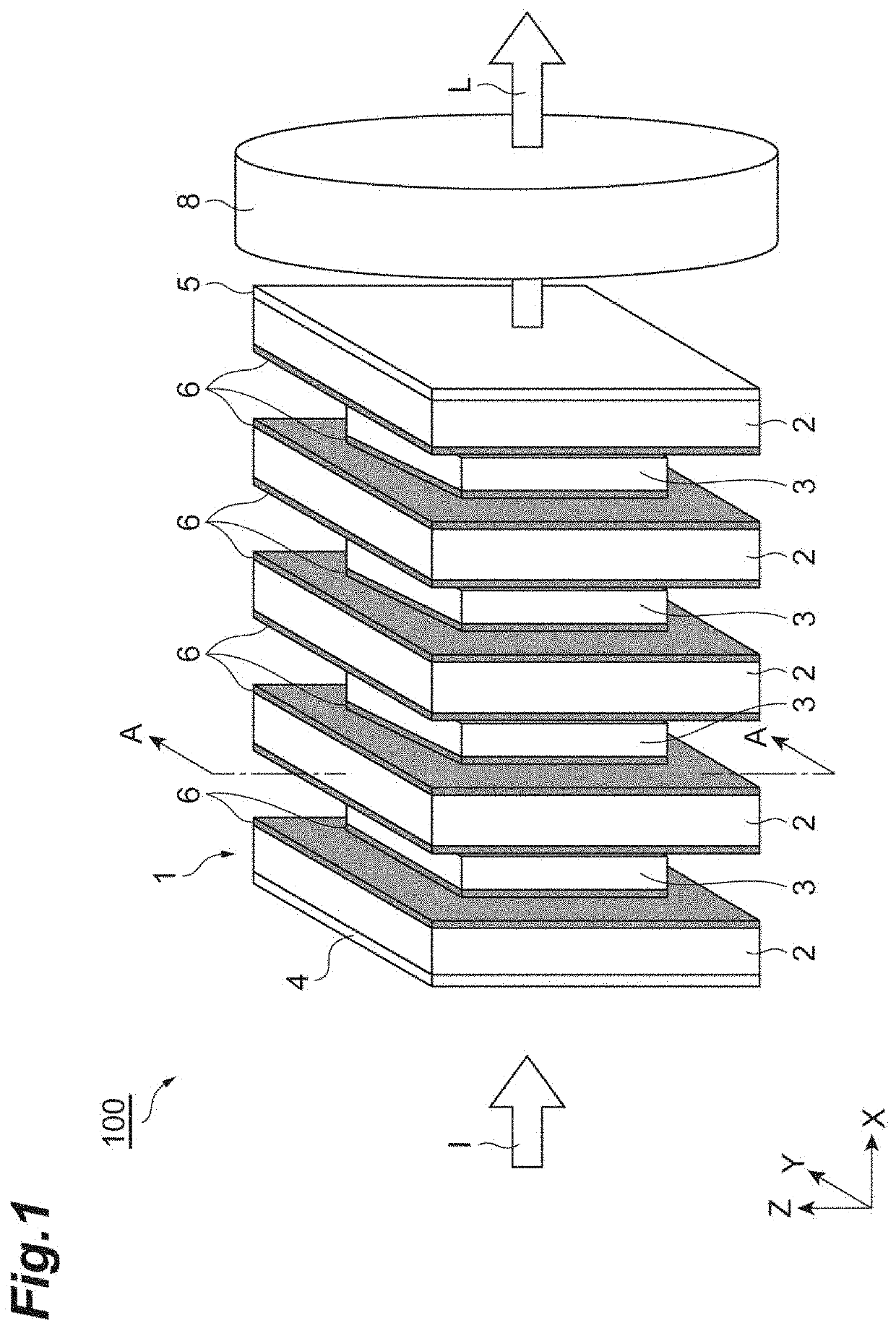
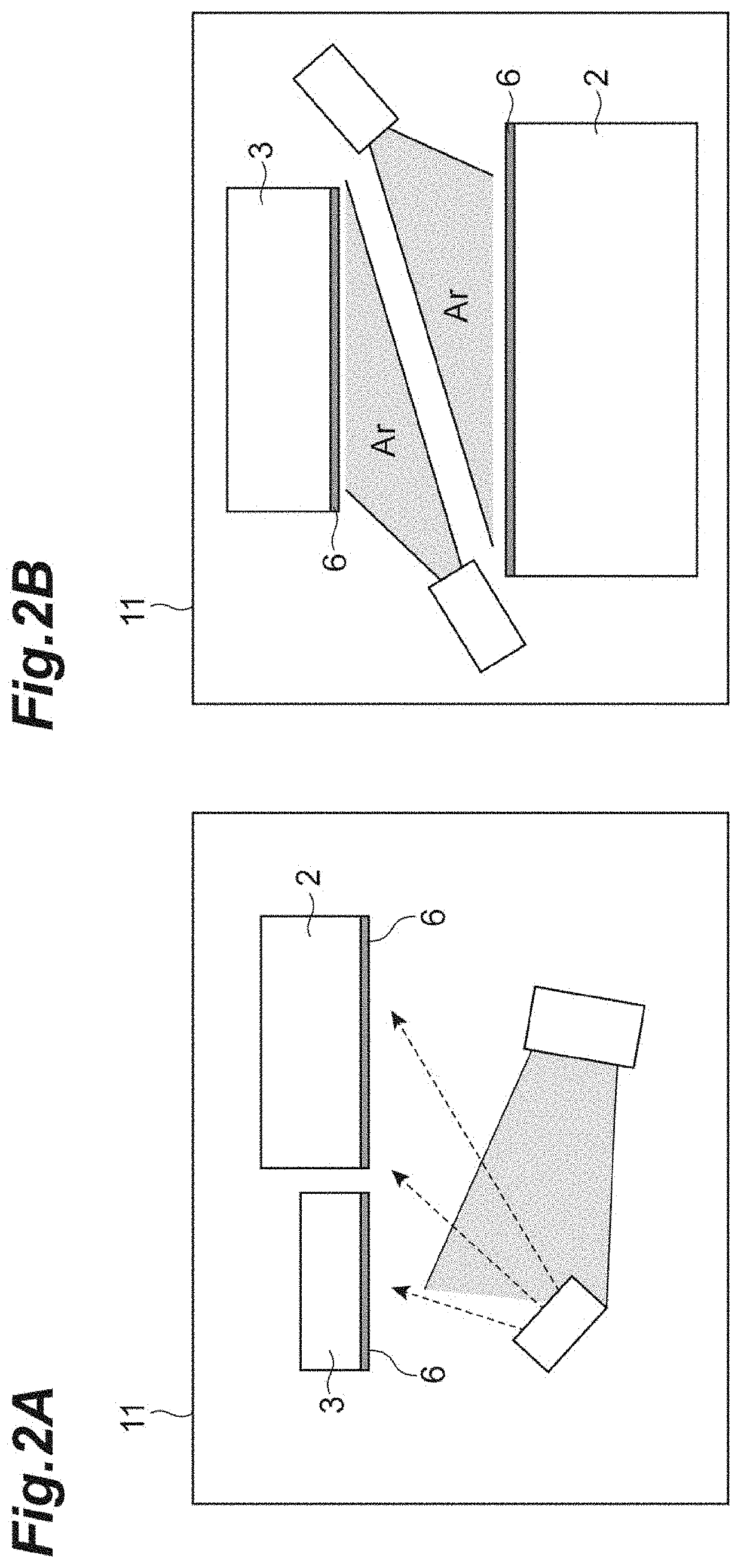
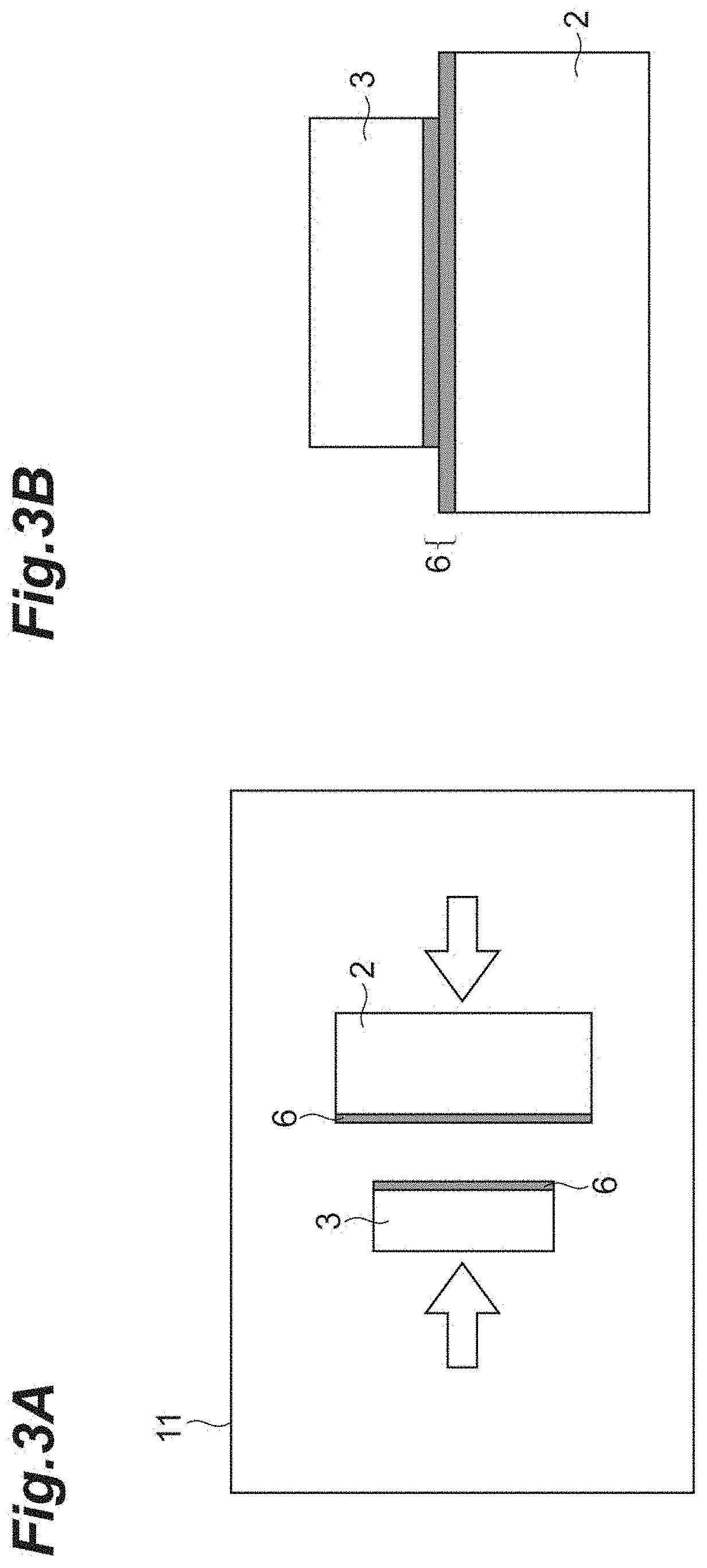
[0143]FIG. 16A to 16D is a longitudinal sectional view showing a nonlinear wavelength conversion element 801 according to the eighth group of example embodiments. The nonlinear wavelength conversion element 801 is an optical element having a periodic structure for performing quasi-phase matching (QPM). When the nonlinear wavelength conversion element 801 is manufactured, a plurality of quartz plates 802 are prepared, and the plurality of quartz plates 802 are bonded so as to overlap one another via an intermediate layer 806 as shown in FIG. 16A. Among the plurality of quartz plates 802, a pair of adjacent quartz plates 802 is disposed so as to have different polarities of target generated electric fields. Quartz has no spontaneous...

configuration example 1

[0157]An optical element including a laser medium, a Q switch element laminated on the laser medium, and an intermediate layer therebetween.

configuration example 2

[0158]An optical element including a transparent heat sink, a laser medium laminated on the heat sink, and an intermediate layer located therebetween.


PUM

PropertyMeasurementUnit
wavelengthaaaaaaaaaa
thicknessaaaaaaaaaa

Abstract

A method for manufacturing an optical element includes a bonding step of bonding a first and a second element portion to each other without interposing an adhesive therebetween. The bonding step includes: a first step of fixing the first and the second element portion with an intermediate layer disposed between these portion, the intermediate layer containing an element substitutable for a constituent element of a bonded portion in the first and the second element portion, the intermediate layer being colored; and a second step of integrating a part of the intermediate layer with the first and the second element portion, and making a part of the intermediate layer transparent to laser light by irradiating the intermediate layer with giant pulse laser light and causing it to be absorbed into the intermediate layer after the first step.

Description

CROSS-REFERENCE TO RELATED APPLICATION[0001]This application claims the benefit of priority from Japanese Patent Application No. 2018-010560, filed Jan. 25, 2018, the entire contents of which are incorporated herein by reference.BACKGROUND1. Technical Field[0002]A method for manufacturing an optical element through which laser light is transmitted or reciprocated, and the optical element.2. Description of the Related Art[0003]As a method for manufacturing an optical element, a method including a step of bonding a first element portion and a second element portion, which are transparent to emitted laser light, to each other without interposing an adhesive therebetween is known. As a technique of this type, for example, a laser element obtained by bonding diamond (second element portion) to Nd:YAG (first element portion) at normal temperature is disclosed in Katsumata, Ichikawa and Shoji, “High-Efficiency and High-Power Operation of Normal-Temperature-Bonded Nd:YAG / Diamond Composite L...

Claims


Application Information

Patent Timeline
Patent Type & Authority Patents(United States)
IPC IPC(8): H01S3/04H01S3/07H01S3/06H01S3/08H01S3/00H01S3/042B29D11/00H01S3/113
CPCH01S3/0085H01S3/0627H01S3/042B29D11/0074B29D11/00865H01S3/0401H01S3/07H01S3/0612H01S3/0805H01S3/0604H01S3/113H01S3/0621H01S3/0623H01S3/0405
Inventor TAIRA, TAKUNORIKAUSAS, ARVYDAS
Owner INTER UNIV RES INST NAT INST OF NATURAL SCI
Why Eureka
Try Eureka