Dimming device, image display device, and display device
a technology of image display and dimming device, which is applied in the direction of color television details, television systems, instruments, etc., can solve the problem that the virtual image observed by the observer cannot be sufficiently contrasted, and achieve the effect of suppressing the phenomenon
- Summary
- Abstract
- Description
- Claims
- Application Information
AI Technical Summary
Benefits of technology
Problems solved by technology
Method used
Image
Examples
example 1
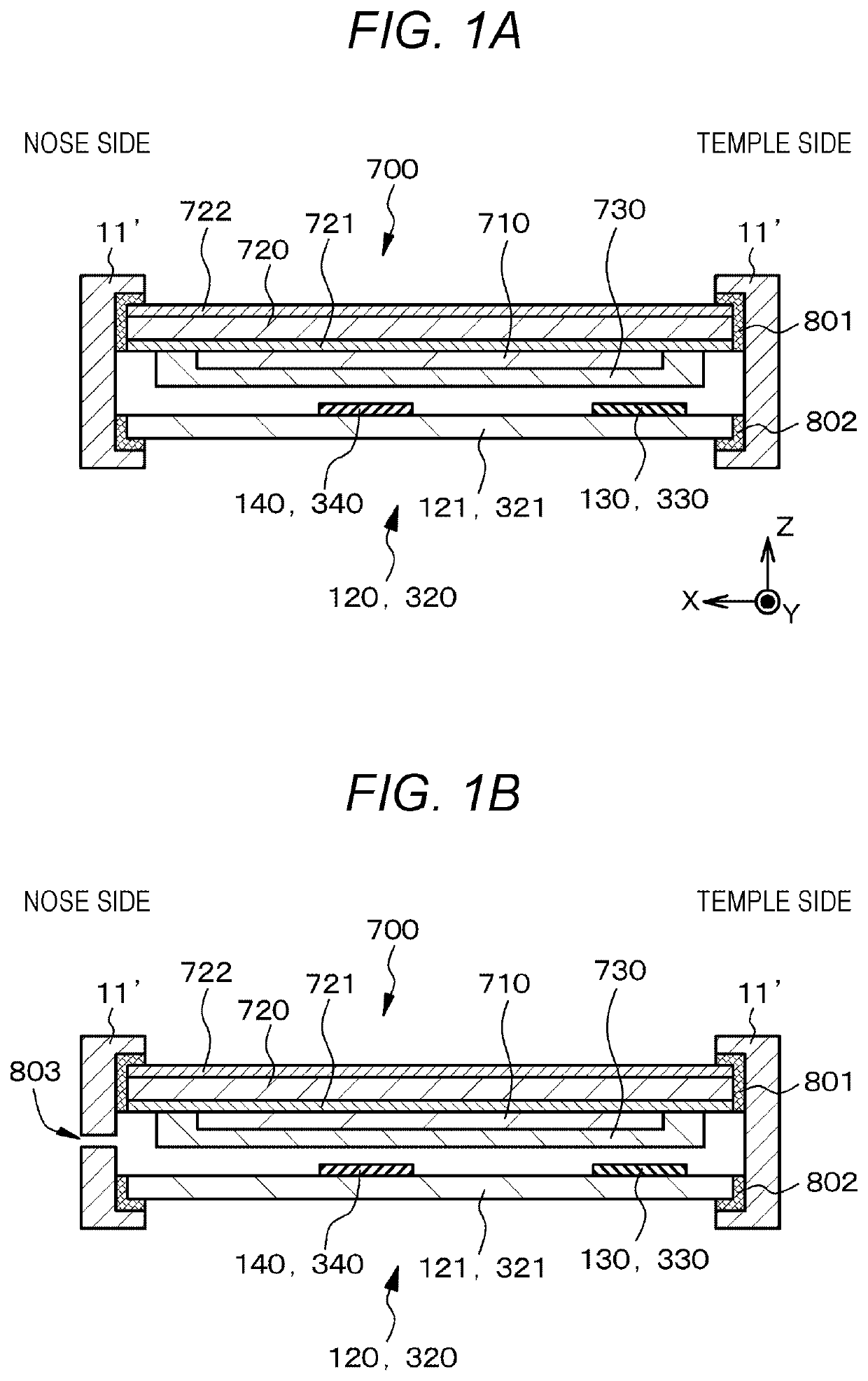
[0133]Example 1 relates to the image display device of the present disclosure and the display device (specifically, head mounted display (HMD)) of the present disclosure, specifically to the optical device with first structure (more specifically, optical device with structure 1-B) and a display device including the image forming device with first configuration. Furthermore, Example 1 relates to the dimming device of the present disclosure. FIG. 1A illustrates a schematic cross-sectional view obtained by cutting a part of the image display device of Example 1 along an XZ plane. FIG. 7A illustrates a schematic view of the dimming device as viewed from the front. FIG. 7B illustrates a schematic cross-sectional view obtained by cutting a part of the image display device of Example 1 along the arrow B-B, that is obtained by cutting a part of the image display device of Example 1 along a YZ plane. Furthermore, FIG. 8A illustrates a schematic partial cross-sectional view of the dimming dev...
example 2
[0194]Example 2 is a modification of Example 1, and relates to the optical device with structure 1-B and the image forming device with second configuration. As illustrated in a conceptual diagram of the image display device 200 in a display device (head mounted display) of Example 2 in FIG. 13, the image forming device 210 of Example 2 is constituted by the image forming device with second configuration. In other words, the image forming device 210 includes a light source 211, a scanning unit 212 for scanning parallel light emitted from the light source 211, and a lens system 213 for converting light emitted from the light source 211 into parallel light. The entire image forming device 210 is housed in a casing 215, and an opening (not illustrated) is formed in the casing 215, and light is emitted from the lens system 213 via the opening. In addition, each casing 215 is detachably attached to each of the temple portions 13 by the attachment member 19. Furthermore, in FIGS. 13, 14, 1...
example 3
[0197]Example 3 is also a modification of Example 1, but relates to the optical device with structure 1-A and the image forming device with first or second configuration.
[0198]As illustrated in a conceptual diagram of the image display device 300 in a display device (head mounted display) of Example 3 in FIG. 14, the first deflecting unit 330 and the second deflecting unit 340 of Example 3 are disposed inside the light guide plate 321. In addition, the first deflecting unit 330 reflects light incident on the light guide plate 321, and the second deflecting unit 340 transmits and reflects light propagated by total reflection through the inside of the light guide plate 321 a plurality of times. In other words, the first deflecting unit 330 functions as a reflecting mirror, and the second deflecting unit 340 functions as a semi-transmissive mirror. More specifically, the first deflecting unit 330 disposed inside the light guide plate 321 is constituted by a light reflecting film (a kin...
PUM
| Property | Measurement | Unit |
|---|---|---|
| thickness | aaaaa | aaaaa |
| thickness | aaaaa | aaaaa |
| temperature | aaaaa | aaaaa |
Abstract
Description
Claims
Application Information


