
Semiconductor device and semiconductor device manufacturing method

a semiconductor device and semiconductor technology, applied in the direction of semiconductor devices, electrical devices, transistors, etc., can solve the problems of thermal destruction, narrow operation range required for esd protection elements, and difficult to realize desired characteristics

Active Publication Date: 2021-09-30
ACCUDX +1
View PDF3 Cites 0 Cited by
  • Summary
  • Abstract
  • Description
  • Claims
  • Application Information

AI Technical Summary

Benefits of technology

The patent text explains that in semiconductor devices, arranging a high-concentration diffusion layer near a gate electrode reduces the breakdown voltage and causes thermal destruction. To prevent this, the high-concentration diffusion layer needs to be moved away from the gate electrode to enhance the breakdown voltage. This results in a region of high concentration between the gate electrode and the drain diffusion layer. A protection element can also enter a bipolar operation by applying an overvoltage, which causes thermal destruction due to the concentration of the electric field at the boundary of the drain diffusion layer. To prevent this, the text suggests creating a region of high concentration in the middle between the gate electrode and the drain diffusion layer. The technical effect of this arrangement is to improve the reliability and stability of semiconductor devices.

Problems solved by technology

However, the operating range required for an ESD protection element is narrowed due to miniaturization, and it is difficult to realize desired characteristics.
In addition, a protection element enters a bipolar operation by applying an overvoltage, and thermal destruction is likely to occur due to the concentration of the electric field at the boundary of the drain diffusion layer.
It has been difficult, however, to manufacture an element capable of protecting an internal element with a margin because a breakdown voltage fluctuates with changes in a structure and process.

Method used


Image

  • Semiconductor device and semiconductor device manufacturing method
  • Semiconductor device and semiconductor device manufacturing method
  • Semiconductor device and semiconductor device manufacturing method

Examples


first embodiment

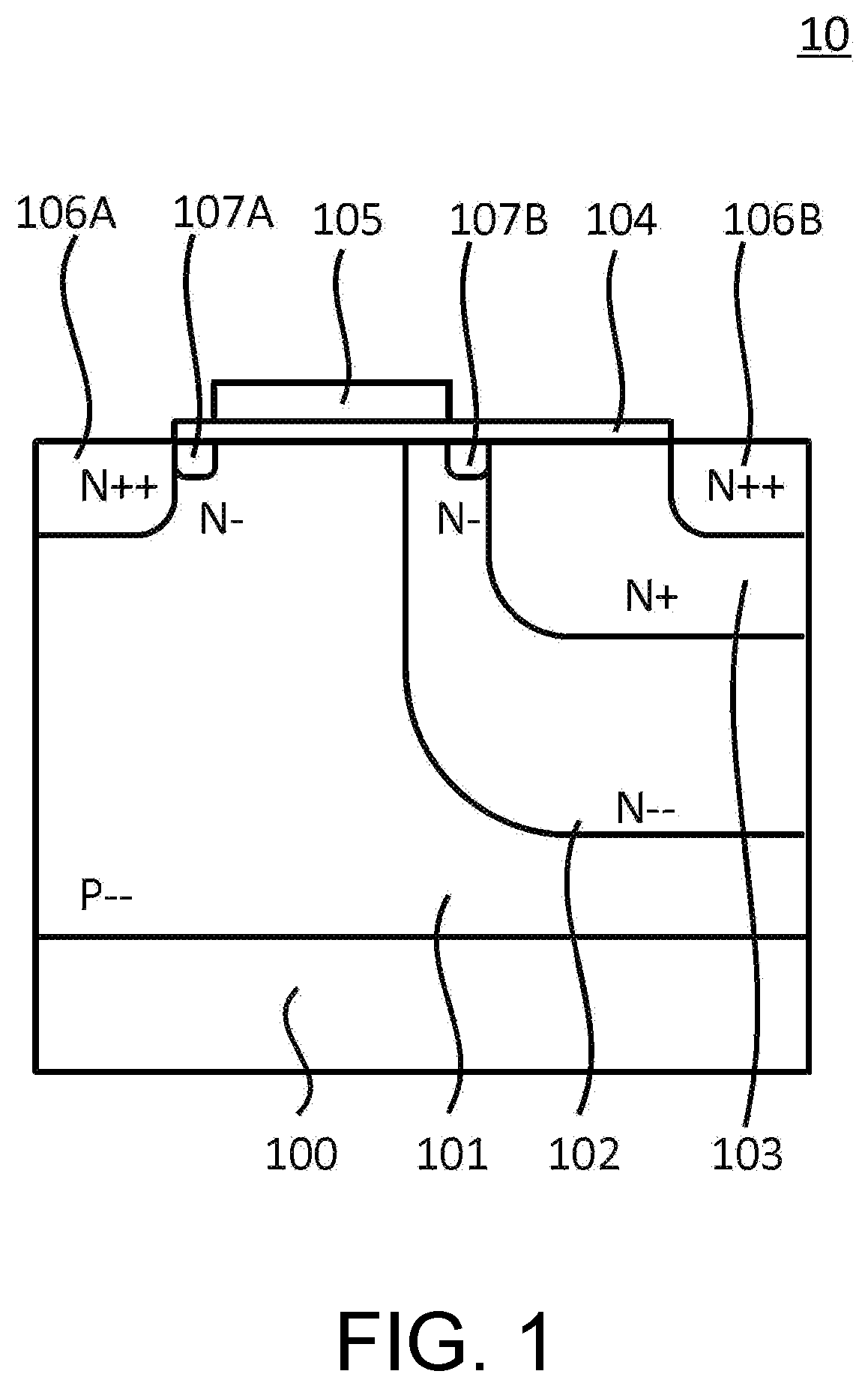
[0033]FIG. 1 is a schematic cross-sectional view illustrating an N-type MOS transistor 10 of a semiconductor device according to a first embodiment of the present invention.

[0034]The N-type MOS transistor 10 includes a semiconductor substrate 100, a second conductivity type (a P-type in the present embodiment) low-concentration diffusion layer 101 disposed inwardly from the surface of the semiconductor substrate 100, a gate electrode 105 disposed on the surface of the semiconductor substrate 100 with an interposition of a gate oxide film 104, a first conductivity type (an N-type in the present embodiment) source diffusion layer 106A disposed on a surface of the semiconductor substrate 100 which is positioned on one side of the gate electrode 105, a first conductivity-type drain diffusion layer 106B disposed on the surface of the semiconductor substrate 100 which is positioned on the other side of the gate electrode 105 to be separated from the gate electrode 105, a first conductivit...

second embodiment

[0053]FIG. 11 is a schematic cross-sectional view illustrating an N-type MOS transistor 50 of a semiconductor device according to a second embodiment of the present invention.

[0054]In the N-type MOS transistor 50, the structure of a drain and a source are the same and symmetrical to each other. That is, in the N-type MOS transistor 10 according to the first embodiment, the structures of the source and the drain are not the same and are asymmetrical to each other, but the N-type MOS transistor 50 is configured by making the structure of a source surrounding a source diffusion layer 106A the same as the structure of a drain.

[0055]Specifically, the N-type MOS transistor 50 includes a semiconductor substrate 100, a second conductivity type (a P-type in the present embodiment) low-concentration diffusion layer 101 disposed inwardly from the surface of the semiconductor substrate 100, a gate electrode 105 disposed on the surface of the semiconductor substrate 100 with an interposition of ...

third embodiment

[0057]FIG. 12 is a schematic cross-sectional view illustrating a P-type MOS transistor 60 of a semiconductor device according to a third embodiment of the present invention. In the P-type MOS transistor 60, conductivity types in all regions in the N-type MOS transistor 10 according to the first embodiment are switched to opposite conductivity types. That is, in the N-type MOS transistor 10, a P-type region is switched to an N-type region, and an N-type region is switched to a P-type region, then we can obtain the P-type MOS transistor 60.

[0058]The P-type MOS transistor 60 includes a semiconductor substrate 100, a second conductivity type (an N-type in the present embodiment) low-concentration diffusion layer 201 disposed inwardly from the surface of the semiconductor substrate 100, a gate electrode 105 disposed on the surface of the semiconductor substrate 100 with an interposition of a gate oxide film 104, a first conductivity type (a P-type in the present embodiment) source diffus...


PUM


Abstract

In the semiconductor device, a high-concentration diffusion layer and a low-concentration diffusion layer are disposed around a drain diffusion layer of an ESD protection element. The high-concentration diffusion layer is separated from a gate electrode, and a medium concentration LDD diffusion layer is disposed in a separation gap. Variations in characteristics are suppressed by reducing thermal treatment on the high-concentration diffusion layer and a medium concentration diffusion layer.

Description

CROSS-REFERENCE TO RELATED APPLICATION[0001]The application is based on Japanese Patent Application No. 2020-061816 filed on Mar. 31, 2020, the content of which is incorporated herein by reference.BACKGROUNDTechnical Field[0002]The present disclosure relates to a semiconductor device, and more particularly to a structure of a semiconductor device having an enhanced breakdown voltage and a method for manufacturing the semiconductor device.Description of Related Art[0003]A semiconductor integrated circuit is provided with an electrostatic discharge (ESD) protection element in order to protect an internal element from noise caused by various surges represented by ESD and fluctuations in a power supply voltage. In particular, the operating range of an ESD protection element, such as an off-transistor disposed in a condition that a gate is normally off, needs to be set higher than the maximum operating voltage of a semiconductor integrated circuit and lower than the breakdown voltage of ...

Claims


Application Information

Patent Timeline
IPC IPC(8): H01L29/78H01L21/225H01L21/265H01L29/66
CPCH01L29/7833H01L29/66492H01L21/26513H01L21/2253H01L29/7835H01L29/0607H01L29/0684H01L29/36H01L27/0266H01L27/0296H01L29/1045H01L29/66659H01L29/7836H01L29/42368H01L29/0847
Inventor HATAKENAKA, MASAHIRO
Owner ACCUDX
Learn More