Die stack structure, semiconductor package having the same and method of manufacturing the same

a technology of semiconductor packaging and stack structure, which is applied in the direction of semiconductor devices, semiconductor/solid-state device details, electrical devices, etc., can solve the problems of small die stack structure production yield and unoptimized mold resin, and achieve the effect of improving the reliability and stability of the semiconductor package, reducing the height and improving the form factor of the die stack structure 90

Active Publication Date: 2021-01-05
SAMSUNG ELECTRONICS CO LTD
View PDF16 Cites 10 Cited by
  • Summary
  • Abstract
  • Description
  • Claims
  • Application Information

AI Technical Summary

Benefits of technology

[0013]According to exemplary embodiments of the inventive concept, the base die 10 and the die stack 50 may be directly bonded into the hybrid bonding structure HB without any gap fill molds, nor any bonding adhesives and bonding structures between the die stack 50 and the base die 10, so that no vertical spacing need be provided between the base die 10 and the die stack 50. In the same way, each component dies 20, 30 and 40 of the die stack 50 may be bonded into the hybrid bonding structure HB without any gap fill molds, nor any bonding adhesives and bonding structures between the component die, so that no vertical spacing is provided between neighboring ones of the component dies 20, 30 and 40. Thus the gap fill defects of the die stack structure 90 may be removed or minimized due to the hybrid bonding structure, thereby increasing the reliability and stability of the semiconductor package 500 having the die stack structure 90.
[0014]In addition, since no vertical spacing is provided with the die stack structure 90, the height of the die stack structure 90 may be reduced as much as the size of the absent vertical spacing(s). Thus, the form factor of the die stack structure 90 may be improved due to the hybrid bonding structure.
[0015]Particularly, the die stack 50 may be separated by the mechanical sawing process and the chip C may be separated by an optical sawing process. The cracks of the reforming spots may grow in the crack direction and the wafer W may be split in the crack direction. Thus, the side surface S of the base die 10 may be formed to be flat and uniform, while the side surface SS of the die stack 50 may be covered by the uneven residual mold 60. Thus, the die stack structure 90 may have different surface roughnesses between a lower side portion (e.g., comprising the smooth side surface S of the base die 10) and an upper side portion (e.g., comprising the rougher uneven residual mold 60 on the side surface SS of the die stack 50). The roughness of the residual mold 60 may be controlled in view of the adhesive strength of the die stack structure 90 to the circuit board.

Problems solved by technology

However, the greater the gap distance between the neighboring same-sized dies, the smaller the production yield of die stack structures.
However, since the wafer comprises semiconductor materials such as silicon (Si) that is completely different from the mold resin, the mechanical sawing process suitable for cutting the mold resin may not be optimal for cutting the wafer comprising the semiconductor materials and various cutting defects may result.

Method used


Image

  • Die stack structure, semiconductor package having the same and method of manufacturing the same
  • Die stack structure, semiconductor package having the same and method of manufacturing the same
  • Die stack structure, semiconductor package having the same and method of manufacturing the same

Examples


Embodiment Construction

[0025]Reference will now be made to example embodiments, which are illustrated in the accompanying drawings, wherein like reference numerals may refer to like components throughout.

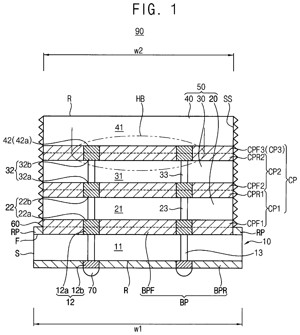
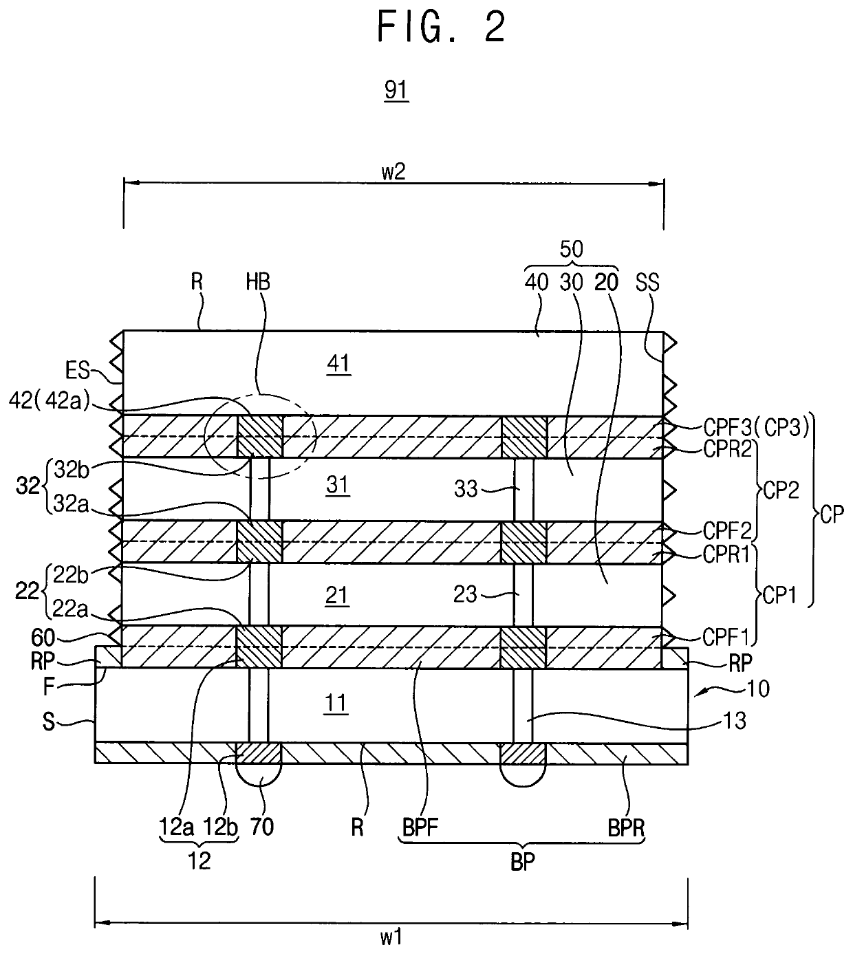
[0026]FIG. 1 is a cross sectional view illustrating a die stack structure in accordance with an example embodiment of the present inventive concept.

[0027]Referring to FIG. 1, a die stack structure 90 in accordance with an example embodiment of the present inventive concept may include a base die 10 having base contact pads 12 insulated by base protection patterns BP and a flat side surface S, a die stack 50 connected to the base die 10 having a plurality of component dies 20, 30 and 40 on the base die 10. Each of the component dies 20, 30 and 40 may include one or more component contact pads 22, 32 and 42 insulated from each other by component protection patterns CP in which they are formed. A residual mold 60 may be unevenly arranged on a side surface SS of the die stack 50. The component dies of the die...


PUM


Abstract

A die stack structure may include a base die having base contact pads insulated by a base protection patterns and a flat side surface, a die stack bonded to the base die and having a plurality of component dies on the base die such that each of the component dies includes component contact pads insulated by a corresponding component protection pattern, and a residual mold unevenly arranged on a side surface of the die stack such that the component dies are attached to each other by the residual mold.

Description

CROSS-REFERENCE TO RELATED APPLICATIONS[0001]This application claims priority under 35 U.S.C. § 119 to Korean Patent Application No. 10-2018-0131220 filed on Oct. 30, 2018 in the Korean Intellectual Property Office, the disclosure of which is incorporated by reference herein in its entirety.BACKGROUND1. Field[0002]Example embodiments relate to a die stack structure, a semiconductor package having the same and a method of manufacturing the die stack structure and the semiconductor package, and more particularly, to a die stack structure having a plurality of hybrid bonded dies, a semiconductor package having the die stack structure and a method of manufacturing the die stack structure and the semiconductor package.2. Description of the Related Art[0003]A die (chip) stack structure has been widely used for increasing the performance and the storage capacity of semiconductor devices. In general, the die stack structure is manufactured by one of a die to die bonding process, wafer to wa...

Claims


Application Information

Patent Timeline
Patent Type & Authority Patents(United States)
IPC IPC(8): H01L25/065H01L23/31H01L23/538H01L23/00H01L23/48H01L21/56H01L21/822
CPCH01L25/0657H01L21/56H01L21/8221H01L23/3128H01L23/3135H01L23/3142H01L23/3185H01L23/481H01L23/5386H01L24/08H01L2224/08145H01L2924/18301H01L21/561H01L21/6836H01L2221/68327H01L23/49827H01L23/49816H01L2224/16227H01L2224/32225H01L2224/73204H01L2224/92125H01L2924/15311H01L2224/06181H01L2224/80203H01L2224/0557H01L2224/0401H01L2224/94H01L2924/3512H01L2224/97H01L2224/05647H01L2224/131H01L24/94H01L24/97H01L24/80H01L24/05H01L24/06H01L24/13H01L24/16H01L24/32H01L24/73H01L25/18H01L2225/06513H01L2225/06517H01L2225/06548H01L2225/06541H01L2224/73251H01L2224/80H01L2924/00014H01L2224/11H01L2924/014H01L2224/16225H01L2924/00H01L2224/08H01L2224/16H01L23/13H01L21/78
Inventor HONG, JI-SEOKKIM, JI-HOONKIM, TAE-HUNLEE, HYUEK-JAEHWANG, JI-HWAN
Owner SAMSUNG ELECTRONICS CO LTD
Why Eureka
Try Eureka