Supercharge Your Innovation With Domain-Expert AI Agents!

Circuit board, package structure and method of manufacturing the same

a technology of circuit boards and package structures, applied in the direction of printed circuits stress/warp reduction, printed circuit non-printed electric components association, printed circuits, etc., can solve the problems of severe warpage issue of multi-layer circuit structures and affect so as to improve the warpage issue of circuit boards and increase the yield rate of package structures

Active Publication Date: 2021-01-19
UNIMICRON TECH CORP
View PDF10 Cites 0 Cited by
  • Summary
  • Abstract
  • Description
  • Claims
  • Application Information

AI Technical Summary

Benefits of technology

[0005]The invention provides a circuit board, a package structure, and a method of manufacturing the same capable of improving the warpage issue of the circuit board and further increasing a yield rate of the package structure.
[0010]To sum up, in the embodiments of the invention, the multilayer structures are formed on the two surfaces of the interconnect substrate, so as to decrease the number of layers of the multilayer structures, thereby improving the warpage issue and increasing the yield rate. In addition, the pattern of the topmost layer in the circuit structures of the multilayer structures is engaged with the pattern of the top surface of the conductive structure of the interconnect substrate, so that the interconnect substrate and the multilayer structures are bonded together, thereby enhancing the reliability.

Problems solved by technology

Nevertheless, when layers in a multilayer circuit structure increase, the warpage issue of the multilayer circuit structure becomes severe.
Further, when the multilayer circuit structure is applied to a package structure, the warpage issue may occur in the package structure as well, and the yield rate of the package structure is thereby affected.

Method used


Image

  • Circuit board, package structure and method of manufacturing the same
  • Circuit board, package structure and method of manufacturing the same
  • Circuit board, package structure and method of manufacturing the same

Examples


first embodiment

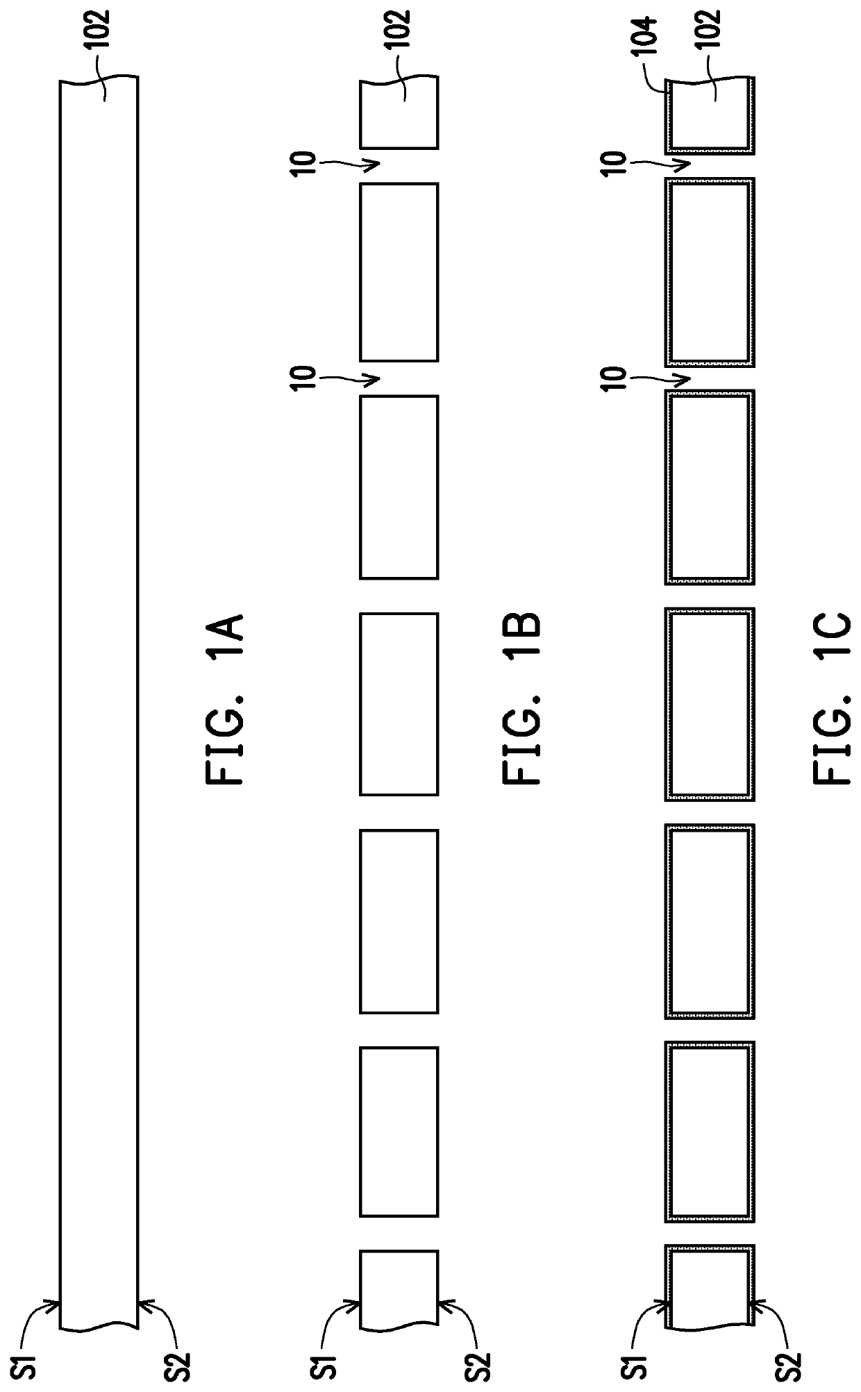
[0022]FIG. 1A to FIG. 1E are schematic cross-sectional diagrams of a manufacturing process of an interconnect substrate according to the invention.

[0023]With reference to FIG. 1A, a core layer 102 is provided, and the core layer 102 has a first surface S1 and a second surface S2 opposite to each other (i.e., two opposite surfaces). In this embodiment, the core layer 102 may be made of prepreg (pp) or other suitable dielectric materials. Nevertheless, in invention is not limited thereto. In other embodiments, the core layer 102 may also be an insulation substrate, a glass substrate, or a combination thereof.

[0024]With reference to FIG. 1B, a plurality of through holes 10 are formed in the core layer 102, so as to communicate with the first surface S1 and the second surface S2 of the core layer 102. That is, the through holes 10 penetrate through the core layer 102 to extend from the first surface S1 of the core layer 102 to the second surface S2 of the core layer 102. In an embodimen...

second embodiment

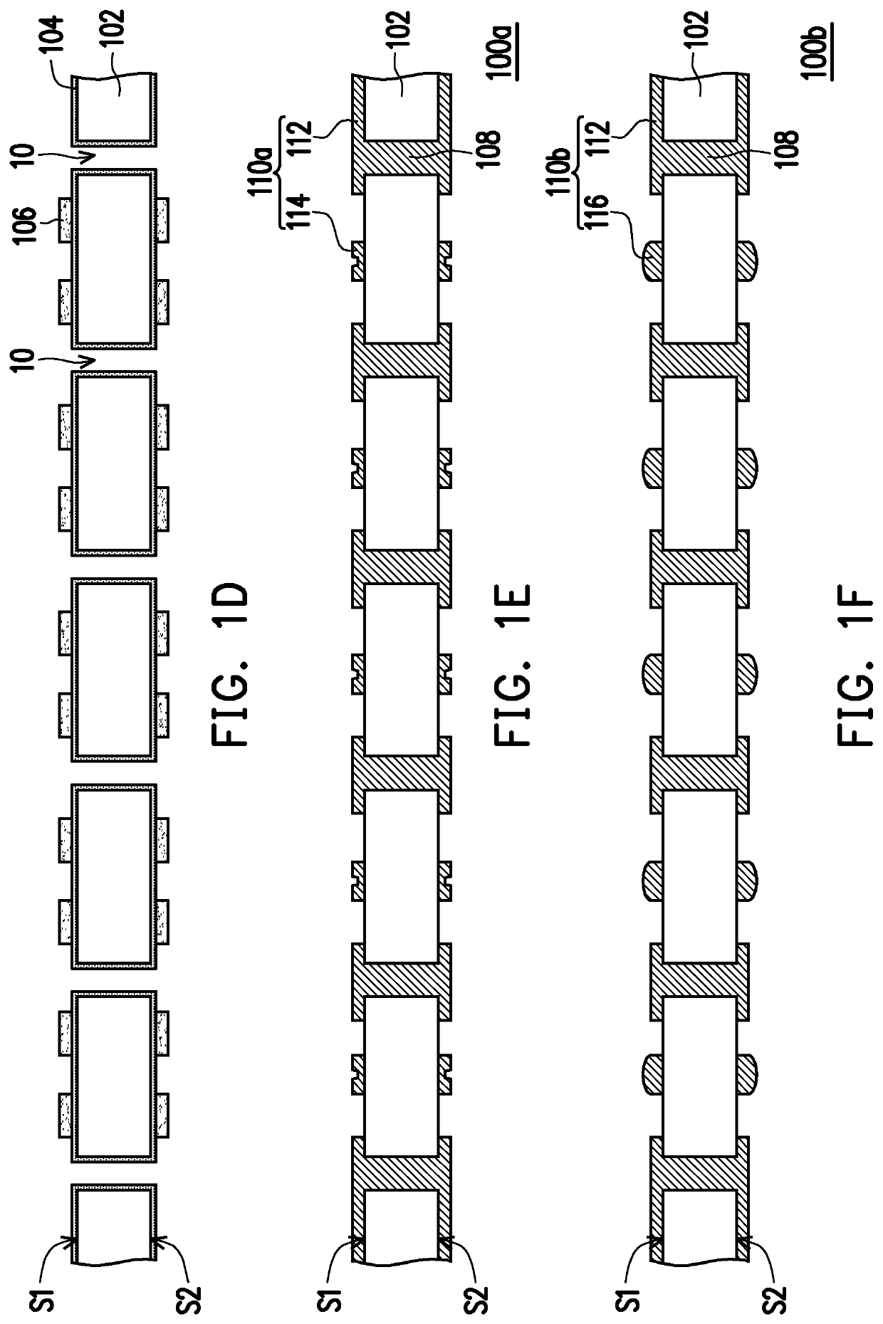
[0030]FIG. 1F is a schematic cross-sectional diagram of an interconnect substrate according to the invention. Note that FIG. 1F depicts a structure which is subsequently formed after the structure of FIG. 1D is formed.

[0031]With reference to FIG. 1D and FIG. 1F, a plating process is performed, so as to form conductive structures 110b respectively on the first surface S1 and the second surface S2 of the core layer 102 and form a plurality of through vias 108 in the through holes 10. Specifically, each of the conductive structures 110b includes a first portion 112 and a second portion 116. As shown in FIG. 1F, the first portion 112 may include a substantially flat top surface, and the second portion 116 has a convex top surface. In this embodiment, the second portion 116 of the conductive structure 110b may be configured to be bonded to the circuit structure 210 (as shown in FIG. 3A). Nevertheless, the invention is not limited thereto. In other embodiments, the first portion 112 may i...

third embodiment

[0058]FIG. 6A to FIG. 6G are schematic cross-sectional diagrams of a manufacturing process of an interconnect substrate according to the invention.

[0059]With reference to FIG. 6A, a core layer 402 is provided, and the core layer 402 has a first surface S1 and a second surface S2 opposite to each other (i.e., two opposite surfaces). In this embodiment, the core layer 402 may be a copper clad laminate (CCL) that has two copper foils 403 disposed on the first surface S1 and the second surface S2 of the core layer 402.

[0060]With reference to FIG. 6B, a plurality of through holes 14 are formed in the core layer 402, so as to communicate with the first surface S1 and the second surface S2 of the core layer 402. That is, the through holes 14 penetrate through the core layer 402 and the two copper foils 403 to extend from the first surface S1 of the core layer 402 to the second surface S2 of the core layer 402. In an embodiment, the through holes 14 may be formed through mechanical drilling...


PUM


Abstract

A circuit board including an interconnect substrate and a multilayer structure is provided. The interconnect substrate includes a core layer and a conductive structure disposed on the core layer. The multilayer structure is disposed on the conductive structure. The multilayer structure includes a plurality of dielectric layers and a plurality of circuit structures. The circuit structures are disposed in the dielectric layers. A topmost layer in the circuit structures is exposed to the dielectric layers to be in contact with the conductive structure. A pattern of the topmost layer in the circuit structures and a pattern of a top surface of the conductive structure are engaged with each other.

Description

CROSS REFERENCE TO RELATED APPLICATION[0001]This application claims the priority benefit of Taiwan application serial no. 107111606, filed on Apr. 2, 2018. The entirety of the above-mentioned patent application is hereby incorporated by reference herein and made a part of specification.BACKGROUNDTechnical Field[0002]The invention relates to a circuit board, a package structure, and a method of manufacturing the same.Description of Related Art[0003]Generally, the multilayer circuit structures of the circuit boards are manufactured by a build-up manner or a lamination manner most of the time, so the multilayer circuit structures may feature high circuit density and reduced circuit pitches. For instance, when a multilayer circuit structure is manufactured, a copper foil and prepreg (pp) are used to constitute a build-up structure first and the build-up structure is repeatedly laminated to be stacked on the core layer, so that the multilayer circuit structure is formed, thereby increasi...

Claims


Application Information

Patent Timeline
Patent Type & Authority Patents(United States)
IPC IPC(8): H05K1/18H05K1/09H05K1/11H05K1/02H05K3/42H05K3/00H05K3/46
CPCH05K1/185H05K1/0271H05K1/09H05K1/115H05K3/007H05K3/429H05K3/4644H01L2224/18H05K3/4614H05K3/4682H05K2203/016H05K2203/061
Inventor TSENG, TZYY-JANGKO, CHENG-TAYANG, KAI-MINGWANG, CHIH-LUN
Owner UNIMICRON TECH CORP
Features
  • R&D
  • Intellectual Property
  • Life Sciences
  • Materials
  • Tech Scout
  • Unparalleled Data Quality
  • Higher Quality Content
  • 60% Fewer Hallucinations
Learn More