
Microdisplay with reduced pixel size and method of forming same

a micro-display and micro-pixel technology, applied in the field of micro-displays, can solve the problems of limiting the shrinkage factor of the oled pixel circuit, the inability to achieve oled-based micro-displays with pixels of only a few microns on the side, and the user's discomfort after prolonged us

Active Publication Date: 2021-03-16
EMAGIN CORP
View PDF14 Cites 0 Cited by
  • Summary
  • Abstract
  • Description
  • Claims
  • Application Information

AI Technical Summary

Benefits of technology

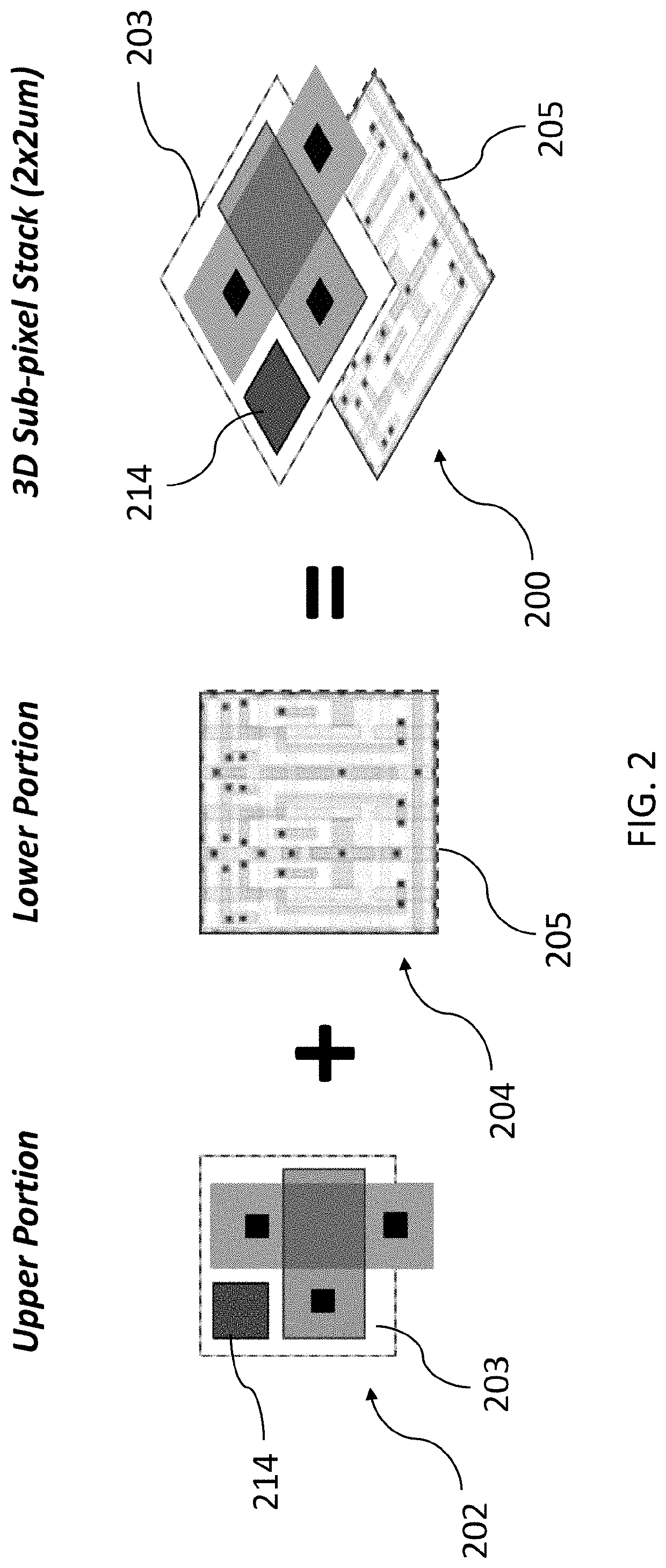
The present invention provides a way to create pixel circuits for microdisplays using a three-dimensional assembly process, which allows for higher pixel densities compared to standard planar processing. This results in smaller, more efficient displays.

Problems solved by technology

A common problem with existing head-mounted display (HMD) systems is user discomfort after prolonged use due to vergence accommodation conflict (VAC).
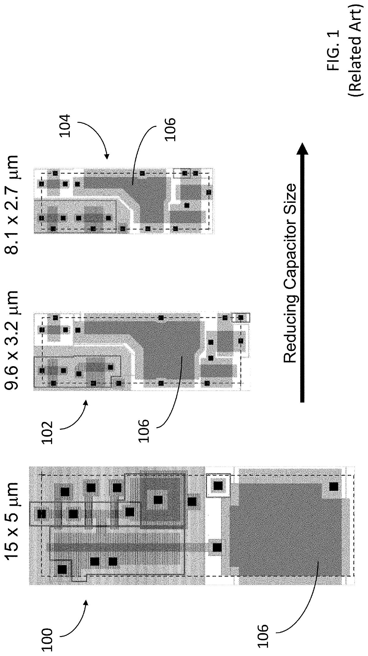
As discussed above, a limiting factor in shrinking the OLED pixel circuit is the required area for components that are built on a conventional planar silicon chip.
Thus, OLED-based microdisplays having pixels of only a few microns on a side are not achievable using existing planar silicon chip fabrication techniques.

Method used


Image

  • Microdisplay with reduced pixel size and method of forming same
  • Microdisplay with reduced pixel size and method of forming same
  • Microdisplay with reduced pixel size and method of forming same

Examples


Embodiment Construction

[0020]In the following detailed description of various embodiments of the system and method of the present invention, numerous specific details are set forth in order to provide a thorough understanding of various aspects of one or more embodiments. However, the one or more embodiments may be practiced without some or all of these specific details. In other instances, well-known methods, procedures, and / or components have not been described in detail so as not to unnecessarily obscure aspects of embodiments.

[0021]While preferred embodiments are disclosed, still other embodiments of the system and method of the present invention will become apparent to those skilled in the art from the following detailed description, which shows and describes illustrative embodiments. As will be realized, the following disclosure is capable of modifications in various obvious aspects, all without departing from the spirit and scope of the present invention. Also, the reference or non-reference to a p...


PUM

PropertyMeasurementUnit
operating voltageaaaaaaaaaa
widthaaaaaaaaaa
areaaaaaaaaaaa

Abstract

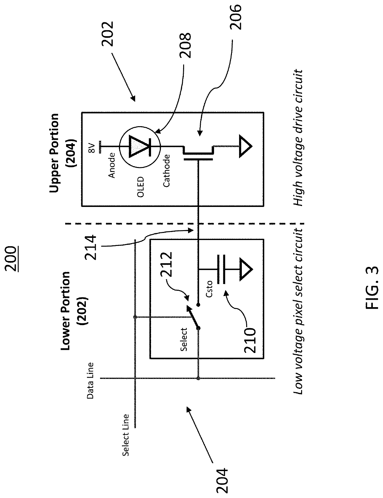
A vertically stacked pixel circuit is provided that includes a high voltage device for driving a pixel on an upper silicon layer, and low voltage circuitry (such as matrix addressing circuitry, data storage circuitry and uniformity compensation circuitry) on a lower silicon layer. The circuitry on the upper and lower silicon layers are electrically connected via a through-silicon via. This unique arrangement allows the high voltage device for driving a pixel to be physically located on top of the larger number of low voltage devices in the lower silicon layer in order to achieve a substantial reduction in overall pixel emission area. The vertically stacked pixel circuit is particularly suited for organic light-emitting diode microdisplays.

Description

STATEMENT OF RELATED CASES[0001]This application claims priority to U.S. Provisional Application Ser. No. 62 / 632,920, filed Feb. 20, 2018, whose entire disclosure is incorporated herein by reference.FIELD OF THE INVENTION[0002]The present invention relates displays in general, and, more particularly, to organic light-emitting diode (OLED) microdisplays with ultra-small pixel sizes.BACKGROUND OF THE INVENTION[0003]There is growing interest in building a display with ultra-small pixel sizes for applications such as virtual reality (VR) to improve the user experience. A common problem with existing head-mounted display (HMD) systems is user discomfort after prolonged use due to vergence accommodation conflict (VAC). Among the various solutions proposed to overcome VAC the most comprehensive is expected to be the light field display.[0004]In the light field approach each pixel comprises multiple sub-pixels, each of which emits directional light. At any particular viewing angle only one ...

Claims


Application Information

Patent Timeline
Patent Type & Authority Patents(United States)
IPC IPC(8): G09G3/3258H01L27/32H01L27/088G09G3/3208H01L27/06H01L21/822
CPCG09G3/3258G09G3/3208H01L21/8221H01L27/0688H01L27/088H01L27/3244G09G2300/0426G09G2300/0465H01L27/3262H10K59/1213H10K59/12
Inventor WACYK, IHOR
Owner EMAGIN CORP
Learn More