Semiconductor device and method for manufacturing the same and wireless communication apparatus

a technology of semiconductor devices and wireless communication devices, which is applied in semiconductor devices, semiconductor/solid-state device details, cooling/ventilation/heating modifications, etc., can solve problems such as mutual interference in metals, failure of operation, etc., and achieve the like generated by electronic components and efficient dissipation of heat generated by electronic components

Active Publication Date: 2021-08-03
MITSUBISHI ELECTRIC CORP
View PDF43 Cites 1 Cited by
  • Summary
  • Abstract
  • Description
  • Claims
  • Application Information

AI Technical Summary

Benefits of technology

[0016]According to the semiconductor device in accordance with the present invention, electromagnetic waves generated from the electronic component can be absorbed by the electromagnetic wave absorption sheet, and heat generated from the electronic component and heat generated from the electromagnetic wave absorption sheet by absorbing the electromagnetic waves can be efficiently dissipated through the heat conduction member including the heat conduction plate and the heat transfer sheet.
[0017]According to the wireless communication apparatus in accordance with the present invention, heat and the like generated from the electronic component can be efficiently dissipated.
[0018]According to the method for manufacturing the semiconductor device in accordance with the present invention, it is possible to manufacture the semiconductor device capable of allowing the electromagnetic wave absorption sheet to absorb electromagnetic waves generated from the electronic component, and efficiently dissipating heat generated from the electronic component and the like through the heat conduction member including the heat conduction plate and the heat transfer sheet.

Problems solved by technology

As operation at higher frequencies is promoted in electronic components, an operation failure may be caused by an electromagnetic wave noise.
In addition, electromagnetic waves generated from the respective electronic components may cause mutual interference within the metal can.

Method used


Image

  • Semiconductor device and method for manufacturing the same and wireless communication apparatus
  • Semiconductor device and method for manufacturing the same and wireless communication apparatus
  • Semiconductor device and method for manufacturing the same and wireless communication apparatus

Examples


first embodiment

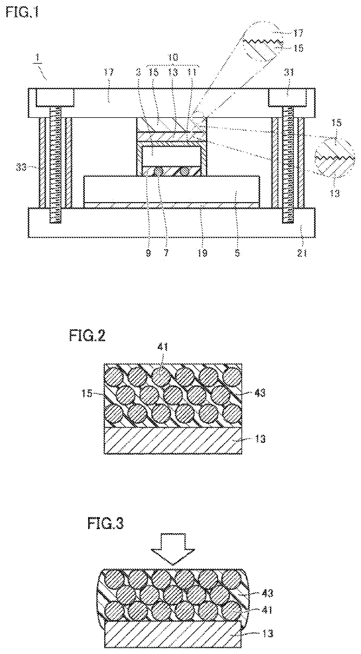
[0043]A semiconductor device in accordance with a first embodiment will be described. As shown in FIG. 1, in a semiconductor device 1, a wiring board 5 is joined to a surface of a supporting member 21 by a bonding layer 19. As bonding layer 19, an electroconductive adhesive, solder, or the like is applied, for example.

[0044]An electronic component 3 is mounted on a surface of wiring board 5. Electronic component 3 is electrically connected to a wire (not shown) formed in wiring board 5 by a solder joint portion 7. A thermosetting resin 9 such as an epoxy resin, for example, is filled into a region between electronic component 3 and wiring board 5 around solder joint portion 7. Thermosetting resin 9 has a function of improving joint reliability of solder joint portion 7.

[0045]An electromagnetic wave absorption sheet 11 is arranged to contact an upper surface and side surfaces of electronic component 3. A heat conduction plate 13 is arranged to contact a portion of electromagnetic wav...

second embodiment

[0100]As a semiconductor device in accordance with a second embodiment, an example of a semiconductor device having a plurality of electronic components mounted on a wiring board will be described.

[0101]As shown in FIG. 13, in semiconductor device 1, a plurality of electronic components 3 are mounted on wiring board 5. Here, two electronic component 3a and 3b are mounted as an example thereof. Electromagnetic wave absorption sheet 11 is arranged to contact an upper surface and side surfaces of each of two electronic components 3a and 3b. Heat conduction plate 13 is arranged to contact upper surfaces of electromagnetic wave absorption sheets 11 in a manner extending over electronic components 3a and 3b. Heat transfer sheet 15 is arranged to contact heat conduction plate 13.

[0102]Heat dissipation member 17 is arranged to contact heat transfer sheet 15. Further, also in this semiconductor device 1, wiring board 5 is joined to a supporting member (not shown), as in the semiconductor dev...

third embodiment

[0107]As a semiconductor device in accordance with a third embodiment, an example of a semiconductor device having a heat conduction plate covering side surfaces and an upper surface of an electronic component will be described.

[0108]As shown in FIG. 14, in semiconductor device 1, electronic component 3 is mounted on wiring board 5. Electromagnetic wave absorption sheet 11 is arranged to contact an upper surface and side surfaces of electronic component 3. A heat conduction plate 14 is arranged to contact a portion of electromagnetic wave absorption sheet 11 covering the side surfaces and the upper surface of electronic component 3. Heat transfer sheet 15 is arranged to contact heat conduction plate 14.

[0109]Next, an example of a method for manufacturing semiconductor device 1 described above will be described. The manufacturing method is basically the same as that in the first embodiment. First, as shown in FIG. 15, electronic component 3 is mounted on the surface of wiring board 5...


PUM


Abstract

An electromagnetic wave absorption sheet is arranged to contact an upper surface and side surfaces of an electronic component mounted on a wiring board, a heat conduction plate is arranged to contact the electromagnetic wave absorption sheet, a heat transfer sheet is arranged to contact the heat conduction plate, and a heat dissipation member is arranged to contact the heat transfer sheet. Heat conductive particles contained in the heat transfer sheet contact a flat surface portion of the heat conduction plate. The electromagnetic wave absorption sheet, the heat conduction plate, and the heat transfer sheet are interposed between the heat dissipation member and the electronic component, as a heat conduction member for conducting heat generated in the electronic component and the like to the heat dissipation member.

Description

TECHNICAL FIELD[0001]The present invention relates to a semiconductor device and a method for manufacturing the same and a wireless communication apparatus. In particular, the present invention relates to a semiconductor device having an electromagnetic wave absorption sheet and a heat transfer sheet, a method for manufacturing such a semiconductor device, and a wireless communication apparatus to which such a semiconductor device is applied.BACKGROUND ART[0002]In recent years, as higher-speed communication and downsizing of electronic apparatuses, in particular, communication apparatuses progress, operation at higher frequencies has been promoted in electronic components such as semiconductor elements. As operation at higher frequencies is promoted in electronic components, an operation failure may be caused by an electromagnetic wave noise. Thus, a method for shielding electromagnetic waves by covering electronic components with a metal can is generally known.[0003]However, in the...

Claims


Application Information

Patent Timeline
Patent Type & Authority Patents(United States)
IPC IPC(8): H01L23/552H01L23/367H01L23/40H01L23/00H05K7/20H01L23/36H05K9/00H01L25/065
CPCH01L23/552H01L23/00H01L23/36H01L23/3675H01L23/40H01L23/4006H05K7/20H05K9/00H01L24/16H01L24/32H01L24/73H01L25/0655H01L2023/4025H01L2023/4087H01L2224/16225H01L2224/32225H01L2224/73204H01L2924/3025H01L23/42H01L23/3737H01L2023/405H01L2023/4056H01L2023/4062H01L2023/4068H01L25/105H01L2224/16227H01L2224/2919H01L2924/00H01L2924/0665
Inventor HAMAGUCHI, TSUNEOTANISHITA, TOMOHIROSATO, SHOTA
Owner MITSUBISHI ELECTRIC CORP
Why Eureka
Try Eureka