Bonding equipment

a technology of equipment and adhesives, applied in the direction of electrical equipment, semiconductor devices, semiconductor/solid-state device details, etc., can solve the problems of easy generation of dust, increased tray and adhesive dust, and difficult dust managemen

Active Publication Date: 2021-10-12
SHARP KK
View PDF19 Cites 2 Cited by
  • Summary
  • Abstract
  • Description
  • Claims
  • Application Information

AI Technical Summary

Benefits of technology

[0006]It is desirable to provide bonding equipment capable of suppressing adhesion of dust to a bonding surface and performing appropriate bonding, and realizing a high yield when bonding a chip, a substrate, and the like having a large number of electrodes to be bonded and small-size electrodes.

Problems solved by technology

When forming such chip / wafer bonding, the following problem occurs.
Therefore, a large amount of dust adheres to the micro LED after the chip forming process.
Since the chip is stored in a tray in many cases and the chips may not be completely fixed in the tray, dust is easily generated during conveyance or the like of the tray and adhesive dust increases.
In either case, dust management is difficult in the process to be in the chip state, and there is a problem that adhesion of various foreign matters may not be avoided.
Further, if a chip to which a large amount of dust or a large number of foreign matters adhere is bonded to a wafer by using existing bonding equipment, dust adheres to a bonding surface and causes a large number of bonding defects, which is a factor of reducing a bonding yield.
Since the bonding defect is conspicuous as an electrode size to be bonded becomes smaller and the number of bonded electrodes increases, the bonding defect is a major problem in production of the display element of the micro LED.

Method used


Image

  • Bonding equipment
  • Bonding equipment
  • Bonding equipment

Examples


first embodiment

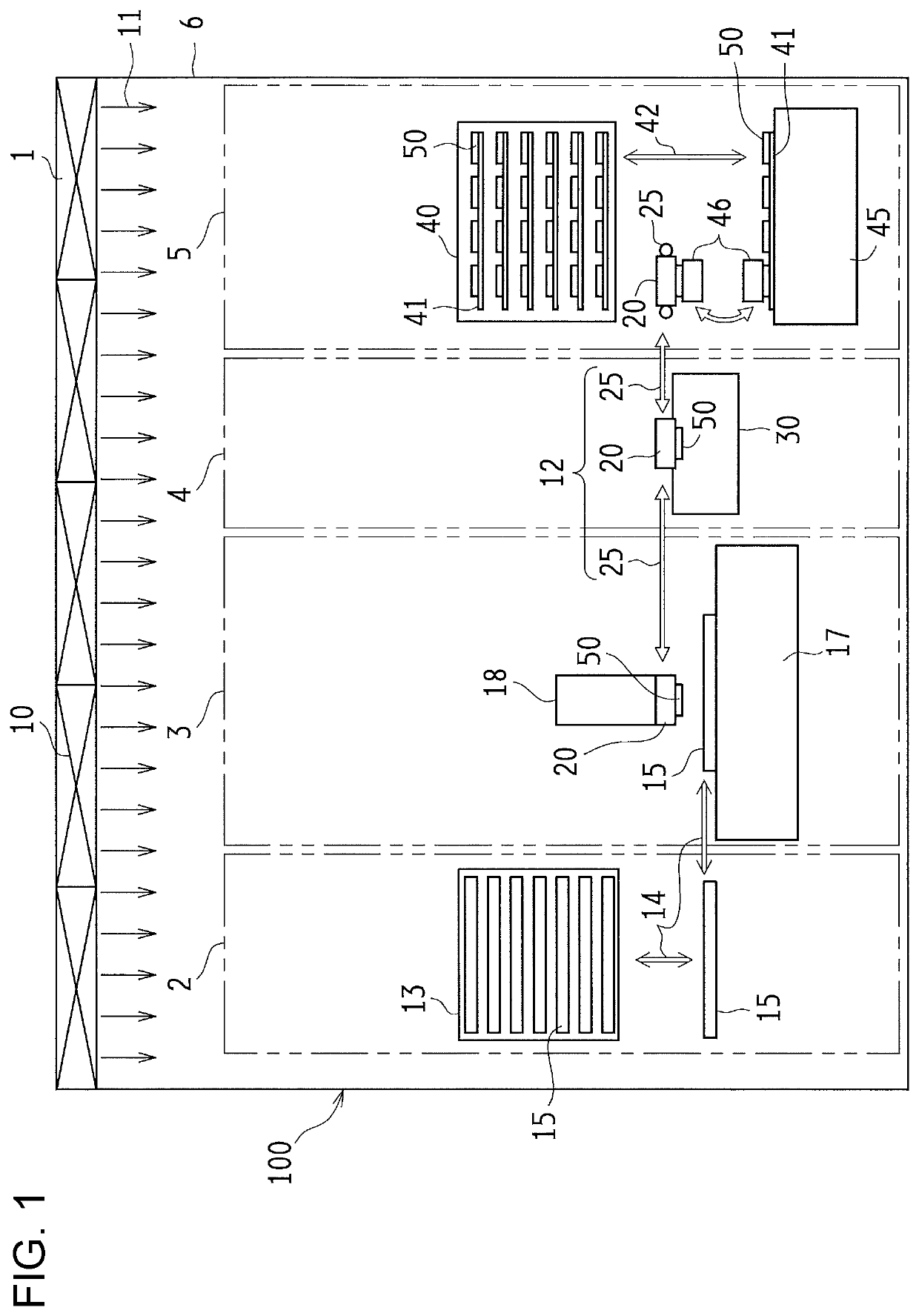
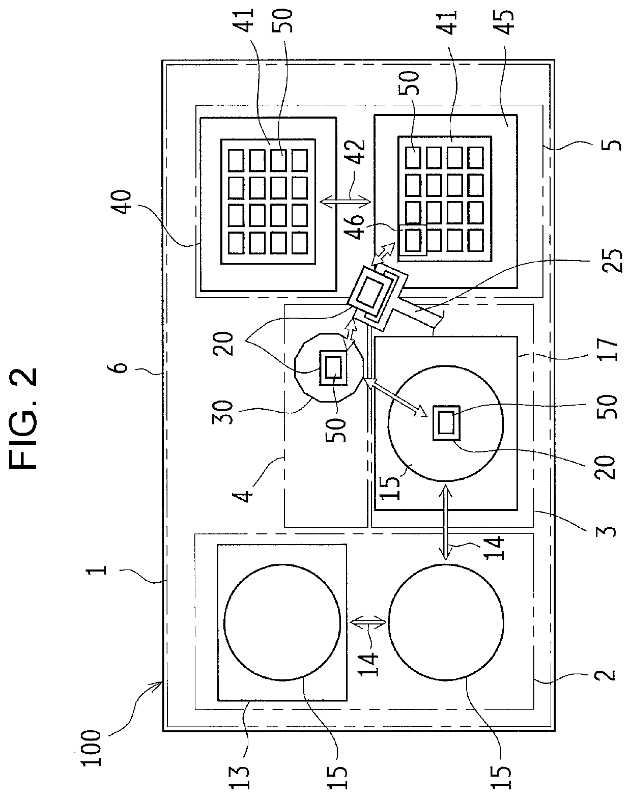
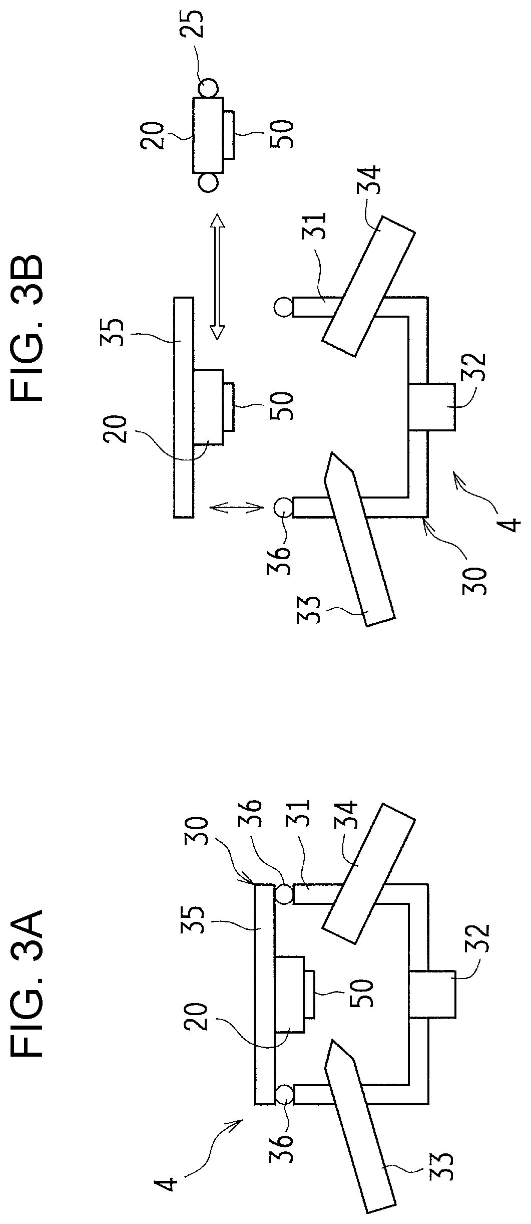
[0021]FIG. 1 illustrates bonding equipment 100 according to the first embodiment of the present disclosure and is a front view illustrating the bonding equipment 100. FIG. 2 is a top view illustrating the bonding equipment 100, and FIGS. 3A and 3B are cross-sectional views illustrating a configuration of a cleaning portion 4 in the bonding equipment 100. In addition, FIGS. 12A to 12D are cross-sectional views schematically illustrating a bonding state of a substrate and a chip.

[0022]Each of the drawings referred to in the following description is a schematic explanatory view illustrating a configuration of the bonding equipment 100 according to the present disclosure, for simplicity, a specific form such as a housing, a transfer portion, or the like will be omitted. In the cross-sectional view in FIGS. 3A and 3B or the like, the cleaning portion 4 in the bonding equipment 100 is schematically illustrated by a cross section, and in order to make the drawing easier to see, hatching il...

second embodiment

[0073]FIGS. 4 and 5 illustrate the bonding equipment 100 according to the second embodiment of the present disclosure. FIG. 4 is a front view illustrating the bonding equipment 100 and FIG. 5 is a top view illustrating the bonding equipment 100.

[0074]In the embodiment described below, since the basic configuration is common with the first embodiment, the common configuration is denoted by the same reference numerals as those in the first embodiment, and a detailed description thereof will be omitted.

[0075]In the first embodiment, the laminar flow source 1 is provided on the ceiling part, and each configuration member is disposed in the laminar flow of the downflow. On the other hand, the bonding equipment 100 according to the present embodiment has a characteristic in the laminar flow source 1, and each configuration member is disposed in a horizontal laminar flow 11h.

[0076]As illustrated in FIGS. 4 and 5, the laminar flow source 1 is disposed on one side of sides of the bonding eq...

third embodiment

[0079]FIGS. 6, 7A, and 7B illustrate the bonding equipment 100 according to the third embodiment of the present disclosure. FIG. 6 is a front view and FIGS. 7A and 7B are cross-sectional views illustrating the cleaning portion 4.

[0080]The bonding equipment 100 according to the third embodiment has a characteristic in a transfer method of the chip 50 and the cleaning chamber 30, as compared with the bonding equipment 100 according to the first embodiment. That is, in the first embodiment, the chip 50 is configured to be transferred and cleaned in a state of being chucked to the bonding head 20, but in the present embodiment, the chip 50 is configured to transferred and cleaned by itself. Such a configuration is suitable for a case where the chip 50 is relatively large, or a case where the non-electrode surface of the chip is smoothly polished and dust generation is small.

[0081]The bonding equipment 100 includes a transfer hand (a second transfer hand) 26 as the transfer mechanism 12....


PUM


Abstract

Bonding equipment includes a laminar flow source, a chip handling portion, a cleaning portion for cleaning a chip, a bonding portion for bonding the chip and a substrate, and a transfer mechanism for transferring the chip from the chip handling portion to the bonding portion. Among these, at least the bonding portion and the cleaning portion are disposed in a laminar flow by the laminar flow source.

Description

BACKGROUND1. Field[0001]The present disclosure relates to bonding equipment which bonds a chip onto a substrate.2. Description of the Related Art[0002]A semiconductor device represented by a large scale integrated circuit (hereinafter, referred to as LSI) is usually mounted on a printed substrate or the like to be used. Another semiconductor chip is mounted on the LSI formed on a silicon wafer and a device in which the LSI and the semiconductor chip are combined functions as a system, so that it is possible to incorporate more complicated functions into one device. A flip chip mounting technique is known as a technique for mounting the semiconductor chip on the wafer. For example, International Publication No. 2013 / 161891 discloses bonding equipment for bonding the semiconductor chip on the wafer by flip chip bonding.[0003]In a process of bonding a micro LED on an LSI on which a driving circuit is formed and manufacturing a minute display device for image projection, in some cases, ...

Claims


Application Information

Patent Timeline
Patent Type & Authority Patents(United States)
IPC IPC(8): H01L21/67H01L21/687H01L21/677H01L21/683H01L23/00
CPCH01L24/74H01L21/67051H01L21/67144H01L21/67718H01L21/67721H01L21/687H01L21/6831H01L24/75H01L2224/7501H01L2224/751H01L2224/8101H01L2224/83009H01L2224/13144H01L2224/2929H01L2224/29299H01L2224/83851H01L2924/3512H01L2924/37001H01L2224/16145H01L2224/16227H01L2224/32145H01L2224/32225H01L2224/73204H01L24/16H01L24/13H01L24/32H01L24/29H01L24/81H01L24/83H01L2224/0401H01L2924/00014H01L2924/00H01L2224/16225
Inventor IGUCHI, KATSUJIMAEGAWA, MASUMISAWAI, KEIICHIHIGASHISAKA, HIROYOSHIMATSUO, TAKANOBU
Owner SHARP KK
Why Eureka
Try Eureka