Holding apparatus for electrostatically holding a component, including a base body joined by diffusion bonding, and process for its manufacture

a technology of electrostatic holding and holding apparatus, which is applied in the direction of electric apparatus, basic electric elements, semiconductor/solid-state device manufacturing, etc., can solve the problems of limited thermal stability of glued clamps, difficult use of ceramic materials in the manufacture and operation of clamps, adhesive bonding, etc., to avoid the disadvantages of conventional techniques, increase geometric and thermal stability, and high precision and/or tolerate applications.

Active Publication Date: 2021-12-14
ASML NETHERLANDS BV
View PDF19 Cites 0 Cited by
  • Summary
  • Abstract
  • Description
  • Claims
  • Application Information

AI Technical Summary

Benefits of technology

[0026]A benefit of the invention is to provide an improved holding apparatus for electrostatically holding a component, in particular a semiconductor wafer, with which disadvantages of conventional techniques are avoided. In particular, the holding apparatus is to be able to be manufactured using a simplified method, should have increased geometric and thermal stability, is to be able to hold a component with high precision and / or tolerate applications at elevated temperatures, in particular above 350° C. Furthermore, a benefit of the invention is to provide an improved method for manufacturing an electrostatic holding apparatus with which disadvantages of conventional techniques are avoided. In particular, the method is to be characterized in particular by simplified manufacturing of the holding apparatus, enabling high accuracy, reproducibility and stability of the clamp design and / or by insensitivity to high temperatures.

Problems solved by technology

Another challenging task is 3D wafer bonding, in which two or more wafers are bonded and contacted.
However, the use of ceramic materials can be challenging in the manufacture and operation of clamps.
Adhesive bonding can be disadvantageous if adhesives continue to polymerize after hardening and thus can guarantee permanent geometric stability to a limited extension only.
Furthermore, the thermal stability of glued clamps is limited.
Glued clamps therefore have limited suitability for many applications in holding of wafers.
A disadvantage of anodic bonding can result from the thermal process conditions of the process and the limited number of suitable materials.
Glass layers between the joining partners are typically used for anodic bonding, but they insulate thermally and thus severely impair the necessary thermal flow within the device.
In addition, electrically conductive glasses, when used as electrodes, are problematic in comparison to ceramic materials, because glasses are relatively soft and not very resistant to abrasion by the semiconductor wafer, so that the precision of the device deteriorates over time.
Since these parts are produced by combining doped and non-doped powders in a hot press and shrinkage occurs during sintering that cannot be determined beforehand, the accuracy of manufacturing the clamp is severely limited.
This disadvantage is the same for devices with wire mesh.
The conventional multi-layer structure of a clamp with several base body plates often results in a long, almost fully serial process chain with high costs, limited yield, high expenditure and high costs due to reworking in production and a long delivery time.
In this case, additionally applied wear protection layers increase the manufacturing effort and they require renewal in regular cycles.
The problems mentioned occur not only in holding apparatuses for holding semiconductor wafers, but also in other applications, such as e. g. in holding apparatuses for holding glass plates.
So far, applications of diffusion bonding have been limited to the connection of joining partners with simple, unstructured surfaces with an extremely high planarity.

Method used


Image

  • Holding apparatus for electrostatically holding a component, including a base body joined by diffusion bonding, and process for its manufacture
  • Holding apparatus for electrostatically holding a component, including a base body joined by diffusion bonding, and process for its manufacture
  • Holding apparatus for electrostatically holding a component, including a base body joined by diffusion bonding, and process for its manufacture

Examples


Embodiment Construction

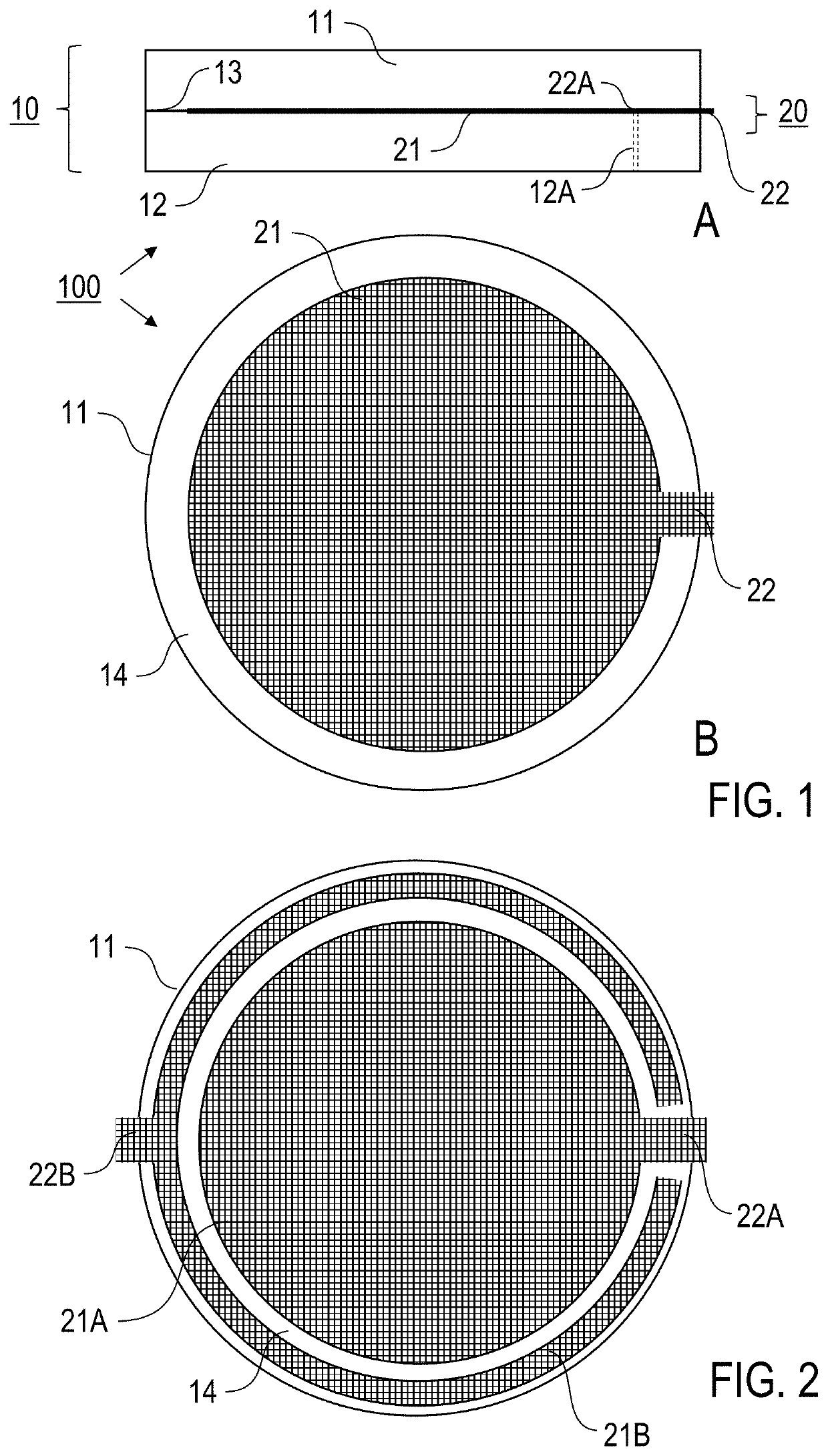
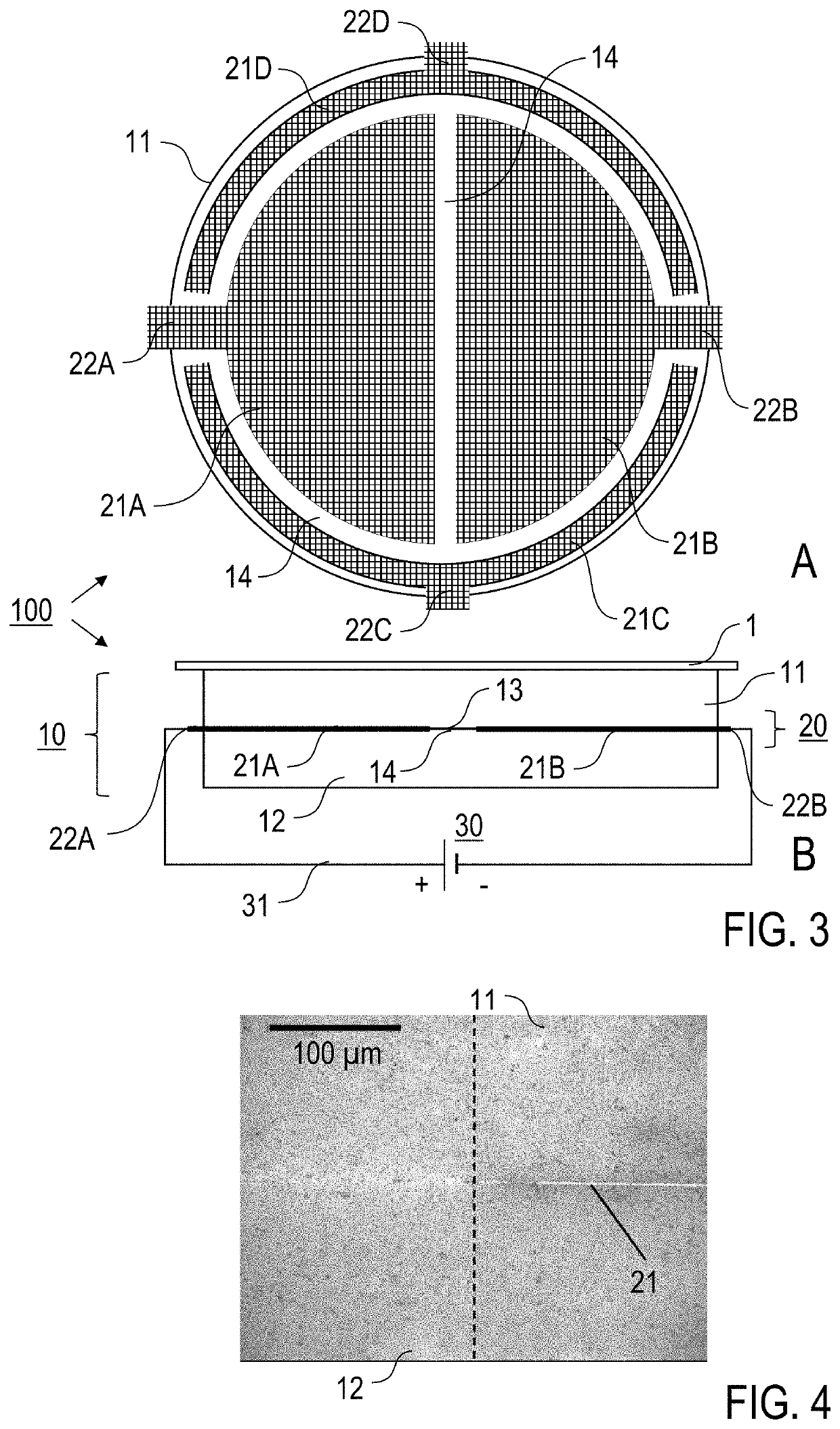
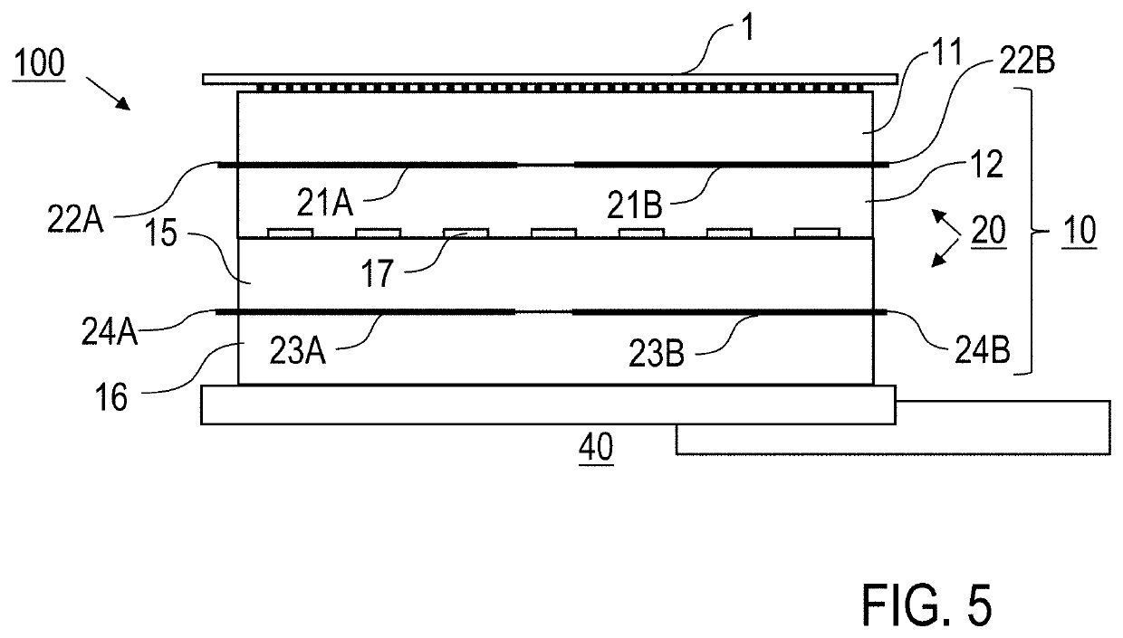
[0035]According to a first general aspect of the invention, the above-mentioned benefit is achieved by an electrostatic holding apparatus for electrostatically holding a component, in particular a semiconductor wafer, such as e. g. a silicon wafer, wherein the electrostatic holding apparatus comprises an electrically insulating, multilayer base body and an electrode device. The base body comprises at least two electrically insulating base body plates (first pair of base body plates), which are connected to one another over a surface by a joint connection. The base body plates are two components which extend in a main plane and preferably have flat surfaces at least on the sides facing one another. The direction along the extension parallel to the main plane is also referred to as the lateral direction and the direction perpendicular thereto as the thickness direction. The base body plates can also be referred to as disks, layers, or sheets. They can each be made in one piece from a ...


PUM


Abstract

A holding apparatus, which is adapted for electrostatically holding a component, in particular a wafer, comprises an electrically insulating base body, which comprises a first pair of base body plates, which are connected to one another in a planar manner via a joint connection, and an electrode device with at least one electrode layer, which is arranged to generate an electrostatic holding force and extends parallel to the extension of the base body plates along the joining connection, wherein the joining connection comprises a diffusion bond connection, wherein the at least one electrode layer is connected in a planar manner to the respectively adjacent base body plate, and the at least one electrode layer has a contact section, which is arranged for electrically contacting the at least one electrode layer. Methods for manufacturing the holding apparatus are also described.

Description

CROSS-REFERENCE TO RELATED APPLICATIONS[0001]This application claims priority to DE 10 2019 101 657.6, filed Jan. 23, 2019, the contents of which are incorporated herein by reference in their entireties for all purposes.BACKGROUND OF THE INVENTION1. Field of Invention[0002]This invention relates to a holding apparatus for electrostatically holding a component, in particular a semiconductor wafer. The invention also relates to methods for manufacturing the holding apparatus. Applications of the invention are available in the provision of equipment or tools for holding components with electrostatic forces, in particular for holding semiconductor wafers, such as e. g. silicon wafers.2. Description of Related Art[0003]In the present description, reference is made to the following prior art, which represents the technical background of the invention. All references cited herein are incorporated herein by reference in their entireties.[0004]U.S. Pat. No. 7,092,231 B2;[0005]U.S. Pat. No. 6...

Claims


Application Information

Patent Timeline
Patent Type & Authority Patents(United States)
IPC IPC(8): H01T23/00H01L21/683
CPCH01L21/6833H01L21/6831
Inventor HOESCHELER, STEFANKIEVEN, DAVIDZIEMANN, MARCELPAMPUCH, CARSTEN
Owner ASML NETHERLANDS BV
Why Eureka
Try Eureka