
Resin multilayer board

a multi-layer board and resin technology, applied in the direction of circuit bendability/stretchability, substantially flat resonant elements, resonance antennas, etc., can solve the problem of difficult control of circuits formed on resin multi-layer boards to have predetermined electrical characteristics, and achieve the effect of reducing the risk of peeling of bonded surfaces and high mechanical strength of mounting surfaces

Active Publication Date: 2022-02-08
MURATA MFG CO LTD
View PDF24 Cites 0 Cited by
  • Summary
  • Abstract
  • Description
  • Claims
  • Application Information

AI Technical Summary

Benefits of technology

This configuration effectively reduces the risk of peeling and maintains predetermined electrical characteristics by distributing stress and enhancing mechanical strength, preventing deformation during mounting and heat processing.

Problems solved by technology

However, with the resin multilayer board described in WO2018 / 100922, when the conductor pattern is formed on the front surface of a resin substrate having recesses and protrusions, it is difficult to control a circuit formed on the resin multilayer board to have predetermined electrical characteristics due to deformation of the conductor pattern.

Method used


Image

  • Resin multilayer board
  • Resin multilayer board
  • Resin multilayer board

Examples


first preferred embodiment

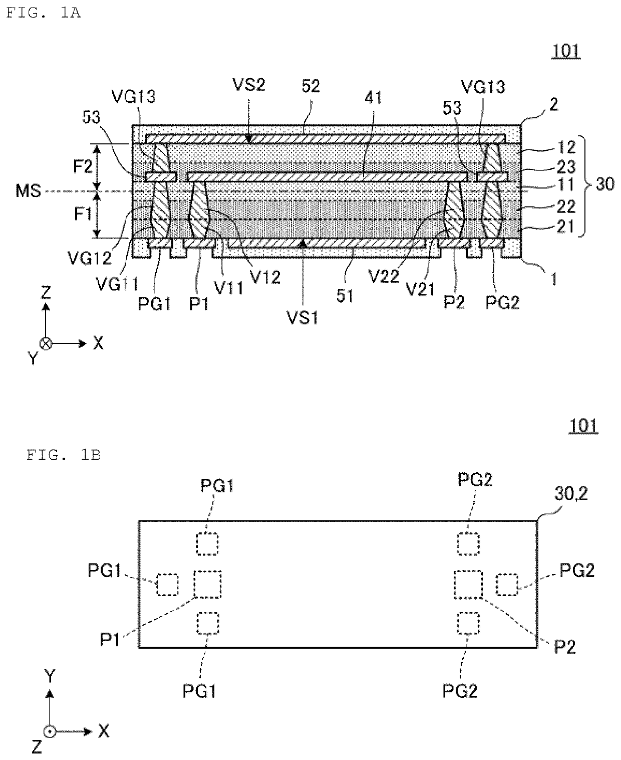
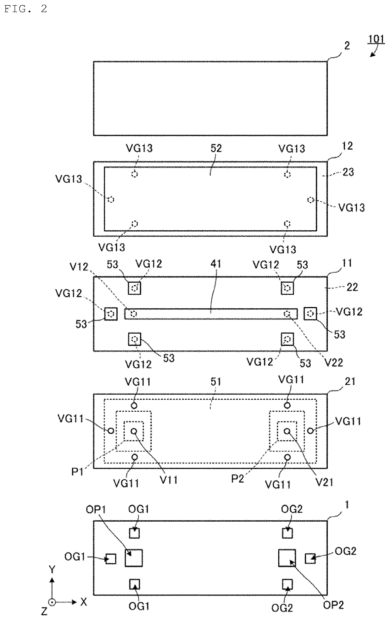
[0022]FIG. 1A is a sectional view of a resin multilayer board 101 according to a first preferred embodiment, and FIG. 1B is a plan view of the resin multilayer board 101. FIG. 2 is an exploded plan view of the resin multilayer board 101.

[0023]The resin multilayer board 101 includes an insulating substrate 30, conductor patterns (a signal conductor pattern 41, ground conductor patterns 51 and 52 and a plurality of connecting conductor patterns 53) provided on a front surface of or inside the insulating substrate 30, mounting electrodes P1 and P2, a plurality of interlayer connecting conductors V11, V12, V21, V22, VG11, VG12, and VG13, protective films 1 and 2, and the like.

[0024]The insulating substrate 30 is a rectangular or substantially rectangular flat plate having a longitudinal direction matching an X-axis direction, and includes a first main surface VS1 and a second main surface VS2 opposite to each other. The insulating substrate 30 is a base body including a thermoplastic re...

second preferred embodiment

[0067]In a second preferred embodiment of the present invention, an example in which a resin multilayer board is connected to a circuit board having a surface with different heights will be described.

[0068]FIG. 5 is a sectional view illustrating a main portion of an electronic device 502 according to the second preferred embodiment.

[0069]The electronic device 502 includes a resin multilayer board 102, a circuit board 402, and the like. As will be described in detail later, the resin multilayer board 102 according to the present preferred embodiment is a transmission line board mounted on another circuit board.

[0070]The resin multilayer board 102 is different from the resin multilayer board 101 according to the first preferred embodiment in that it is bent (having bent portions FP1 and FP2). The resin multilayer board 102 is further different from the resin multilayer board 101 in that connectors 61 and 62 are provided. Other configurations of the resin multilayer board 102 are the s...

third preferred embodiment

[0079]In a third preferred embodiment of the present invention, an example in which a resin multilayer board connects two circuit boards to each other is described.

[0080]FIG. 6 is an external perspective view of a resin multilayer board 103 according to the third preferred embodiment.

[0081]FIG. 7 is a sectional view of the resin multilayer board 103.

[0082]The resin multilayer board 103 includes an insulating substrate 30A, a signal conductor pattern 41, conductor patterns 42 and 43, a ground conductor pattern 51a, mounting electrodes P1, P2, and P3, interlayer connecting conductors V11, V21, V31, V32, and V33, protective films 1a and 1b, and the like.

[0083]Hereinafter, portions different from the resin multilayer board 101 according to the first preferred embodiment will be described.

[0084]The resin multilayer board 103 includes a main body portion BP, a connection portion CN, and a line portion SL. The main body portion BP and the connection portion CN are portions connected to ano...


PUM

PropertyMeasurementUnit
relative permittivityaaaaaaaaaa

Abstract

A resin multilayer board includes an insulating substrate including a first main surface and mounting electrodes only on the first main surface. The insulating substrate includes first and second resin layers that are laminated. The Young's modulus of the second resin layers is higher than that of the first resin layers. The first and second resin layers are arranged in a distributed manner along a lamination direction of the first and second resin layers. The insulating substrate includes a first and second portions that are two equally divided portions of the insulating substrate in the lamination direction and are respectively positioned closer to the first main surface and farther from the first main surface, and a volume ratio of the second resin layers in the first portion is higher than a volume ratio of the second resin layers in the second portion.

Description

CROSS REFERENCE TO RELATED APPLICATIONS[0001]This application claims the benefit of priority to Japanese Patent Application No. 2018-181111 filed on Sep. 27, 2018 and is a Continuation Application of PCT Application No. PCT / JP2019 / 037926 filed on Sep. 26, 2019. The entire contents of each application are hereby incorporated herein by reference.BACKGROUND OF THE INVENTION1. Field of the Invention[0002]The present invention relates to a resin multilayer board, and more particularly, to a resin multilayer board including a plurality of different resin substrates.2. Description of the Related Art[0003]Conventionally, a resin multilayer board has been known that includes an insulating substrate formed by laminating a plurality of resin layers having different elastic moduli, and a conductor pattern formed on the resin substrate.[0004]For example, WO2018 / 100922 discloses a resin multilayer board having a structure formed by laminating a first resin layer and a second resin layer, in which...

Claims


Application Information

Patent Timeline
Patent Type & Authority Patents(United States)
IPC IPC(8): H05K1/03H05K1/02H05K1/14H05K1/16H01Q9/04
CPCH05K1/036H05K1/0271H05K1/0278H05K1/147H05K1/16H01Q9/0407H05K2201/015H05K2201/0141H05K2201/10098H01Q1/38H05K3/4691H05K3/4617H05K1/115H05K2201/096H05K2201/09527H05K2201/098H05K3/4688
Inventor NAGAI, TOMOHIROTAGO, SHIGERU
Owner MURATA MFG CO LTD
Learn More