
Electronic component

a technology of electronic components and components, applied in the field of electronic components, can solve the problems of affecting the balance of the balance of the balance, affecting the q value of the electronic component, and the noise-source electronic component may have an unfavorable influence on other electronic components near the noise-source electronic component, so as to reduce or prevent reducing or preventing the effect of q value reduction

Active Publication Date: 2022-03-15
MURATA MFG CO LTD
View PDF14 Cites 0 Cited by
  • Summary
  • Abstract
  • Description
  • Claims
  • Application Information

AI Technical Summary

Benefits of technology

This configuration reduces the decrease in Q value while maintaining the shielding effect, as the non-shielded areas allow magnetic flux to pass through, thereby reducing eddy currents and insertion loss.

Problems solved by technology

Accordingly, in a case in which noise generated inside the electronic component leaks to the outside, the noise may have an unfavorable influence on other electronic components near the noise-source electronic component.
In a case in which this magnetic flux is blocked by one shield electrode that covers substantially the whole area of each of the component surfaces as described in Japanese Unexamined Patent Application Publication No. 9-121093, an eddy current is generated in the shield electrode so that the insertion loss of the electronic component increases, which may cause a Q value of the electronic component to deteriorate.

Method used


Image

  • Electronic component
  • Electronic component
  • Electronic component

Examples


first preferred embodiment

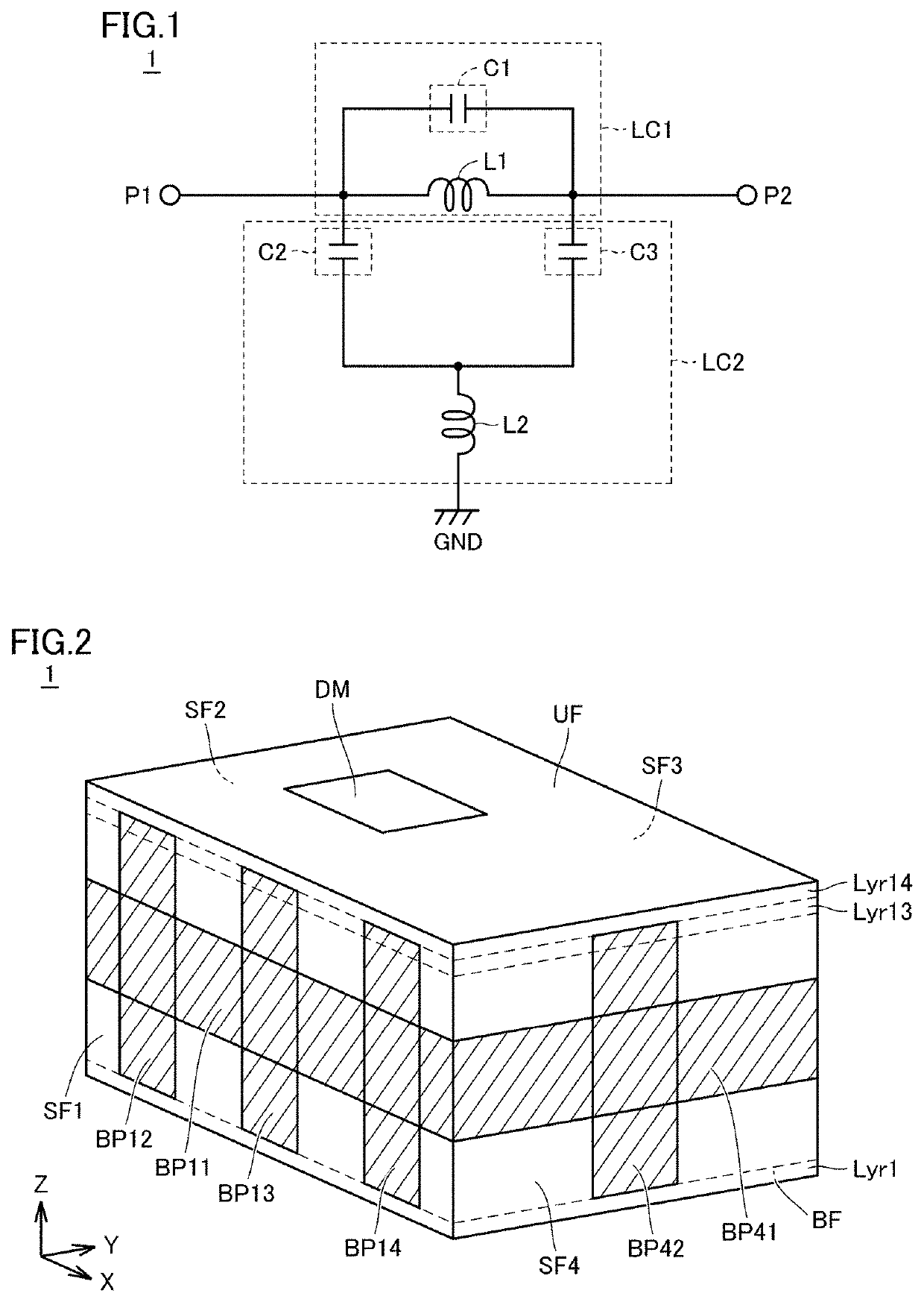
[0038]FIG. 1 is a circuit diagram of a low pass filter 1 as an example of an electronic component according to a first preferred embodiment of the present invention. The low pass filter 1 is an electronic component mounted on a circuit board, and a circuit pattern corresponding to the circuit illustrated in FIG. 1 is provided inside the low pass filter 1. As illustrated in FIG. 1, the low pass filter 1 includes an input-output terminal P1, an input-output terminal P2, an LC parallel resonator LC1, and an LC series resonator LC2.

[0039]The LC parallel resonator LC1 includes an inductor L1 and a capacitor C1. The inductor L1 is connected between the input-output terminal P1 and the input-output terminal P2. The capacitor C1 is connected in parallel to the inductor L1, between the input-output terminal P1 and the input-output terminal P2.

[0040]The LC series resonator LC2 includes an inductor L2, a capacitor C2, and a capacitor C3. One end of the inductor L2 is connected to a ground poin...

second preferred embodiment

[0103]In the first preferred embodiment, the winding axis of the inductor inside the electronic component is parallel or substantially parallel to the lamination direction. In a second preferred embodiment, a case in which a winding axis of an inductor inside an electronic component is perpendicular or substantially perpendicular to the lamination direction will be described.

[0104]FIG. 18 is a circuit diagram of a band pass filter 2 as an example of an electronic component according to a second preferred embodiment of the present invention. The band pass filter 2 is an electronic component that is mounted on a circuit board and includes a circuit pattern corresponding to the circuit illustrated in FIG. 18 therein.

[0105]As illustrated in FIG. 18, the band pass filter 2 includes an input-output terminal P21, an input-output terminal P22, an LC parallel resonator LC21, an LC parallel resonator LC22, an LC parallel resonator LC23 and a capacitor C33.

[0106]The LC parallel resonator LC21 ...

third preferred embodiment

[0139]In the first preferred embodiment and the second preferred embodiment, a case in which a plurality of band-shaped conductor patterns are disposed on shield surfaces so as to define non-shielded areas is provided. The non-shielded area may be provided without using a plurality of band-shaped conductor patterns. In a third preferred embodiment, a case will be described in which a plurality of holes are provided in a planar shield electrode so as to define a non-shielded area.

[0140]A third preferred embodiment of the present invention differs from the first preferred embodiment in that a plurality of holes are provided in a planar shield electrode so as to define a non-shielded area. Since the remaining configuration is the same as or similar to that of the first preferred embodiment, description thereof will not be repeated.

[0141]FIG. 22 is an external appearance perspective view of a low pass filter 3 as an example of an electronic component according to the third preferred emb...


PUM

PropertyMeasurementUnit
frequencyaaaaaaaaaa
magnetic fluxaaaaaaaaaa
areaaaaaaaaaaa

Abstract

An electronic component includes a multilayer body including dielectric layers, a circuit pattern, and band-shaped conductor patterns. The circuit pattern includes a conductor pattern that is disposed inside the multilayer body and defines an inductor. The band-shaped conductor patterns are grounded and cover a portion of a shield surface. An internal surface is located between the circuit pattern and an upper surface. On a shield surface, a non-shielded area is provided which is not covered with any of the band-shaped conductor patterns, and through which magnetic flux generated from the inductor is able to pass.

Description

CROSS REFERENCE TO RELATED APPLICATIONS[0001]This application claims the benefit of priority to Japanese Patent Application No. 2016-176944 filed on Sep. 9, 2016 and is a Continuation Application of PCT Application No. PCT / JP2017 / 026771 filed on Jul. 25, 2017. The entire contents of each of these applications are hereby incorporated herein by reference.BACKGROUND OF THE INVENTION1. Field of the Invention[0002]The present invention relates to electronic components including shield electrodes.2. Description of the Related Art[0003]Electronic components of an integrated circuit are disposed close to each other on a substrate in many cases. Accordingly, in a case in which noise generated inside the electronic component leaks to the outside, the noise may have an unfavorable influence on other electronic components near the noise-source electronic component.[0004]In order to prevent such a situation, a shield electrode is formed on a surface of an electronic component in some cases, as i...

Claims


Application Information

Patent Timeline
Patent Type & Authority Patents(United States)
IPC IPC(8): H01F27/28H01F17/00H03H7/01H03H7/03H05K9/00H01F27/36H01F27/24H03H1/00H01F27/29
CPCH01F27/2885H01F17/0013H01F27/24H01F27/2804H01F27/363H03H1/00H03H7/0115H03H7/03H03H7/1725H03H7/1758H03H7/1766H05K9/00H01F27/29H01F2017/008H01F2027/2809H03H2001/0085H03H2001/0092
Inventor MIYAHARA, KUNIHIROMASUDA, YUTAKAMOTOKI, KANTANAGUMO, SHOJI
Owner MURATA MFG CO LTD
Features
  • Generate Ideas
  • Intellectual Property
  • Life Sciences
  • Materials
  • Tech Scout
  • Unparalleled Data Quality
  • Higher Quality Content
  • 60% Fewer Hallucinations
Learn More