Optoelectronic semiconductor device having a side face as mounting side

a technology of optoelectronic semiconductor and mounting side, which is applied in the direction of semiconductor devices, semiconductor/solid-state device details, electrical equipment, etc., can solve the problem that the requirements cannot be achieved easily with conventional designs

Active Publication Date: 2022-03-15
OSRAM OLED
View PDF17 Cites 0 Cited by
  • Summary
  • Abstract
  • Description
  • Claims
  • Application Information

AI Technical Summary

Benefits of technology

[0004]One object is to specify an optoelectronic semiconductor device, which is distinguished by a low mounting height and permits efficient production of a light current adequate for the use of the device. Furthermore, a method is to be specified with which such optoelectronic semiconductor devices can be produced simply and inexpensively.
[0007]According to at least one embodiment of the optoelectronic semiconductor device, a radiation exit surface of the semiconductor device runs parallel to the active region, thus parallel to a main extension plane of the active region. In particular, the optoelectronic semiconductor device has precisely one radiation exit surface. For example, the radiation exit surface is formed level. “Level” in this context means in particular that the radiation exit surface is free of kinks. However, the level radiation exit surface can be provided with patterning, for example, roughening, to increase the outcoupling efficiency.
[0020]According to at least one embodiment of the semiconductor device, the molding adjoins the semiconductor chip at least at two side faces, in particular at least at two opposing side faces of the semiconductor chip. Furthermore, the molding can also encapsulate all side faces of the semiconductor chip, at least in places. A mechanically stable connection between molding and semiconductor chip is thus simplified.
[0024]According to at least one embodiment of the semiconductor device, the contact track is led over an interface between the molding and the semiconductor chip, wherein the contact track is spaced apart from the interface in a direction running perpendicular to the radiation exit surface. The interface adjoins the front side of the molding in particular. At the interface between the molding and the semiconductor chip, the contact track is not in direct mechanical contact with the semiconductor chip. The danger of an electrical short circuit is thus avoided.
[0029]According to at least one embodiment of the method, the method comprises a step in which an in particular electrically conductive coating is formed on the molding assembly for electrical contacting of the semiconductor chips. The coating is formed patterned for the contacting of the semiconductor chips, thus not over the entire surface. The coating can be formed, for example, by vapor deposition or sputtering. In a later step, the thickness of the electrically conductive coating can be increased, in particular to increase the electrical conductivity, for example, by electrodeposition or electroless deposition.

Problems solved by technology

These requirements cannot be achieved easily with conventional designs.

Method used


Image

  • Optoelectronic semiconductor device having a side face as mounting side
  • Optoelectronic semiconductor device having a side face as mounting side
  • Optoelectronic semiconductor device having a side face as mounting side

Examples


Embodiment Construction

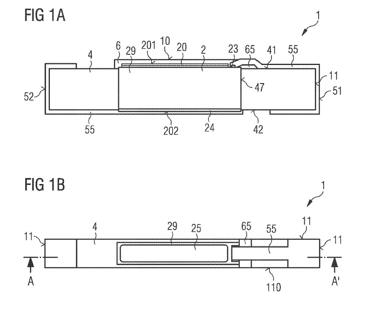
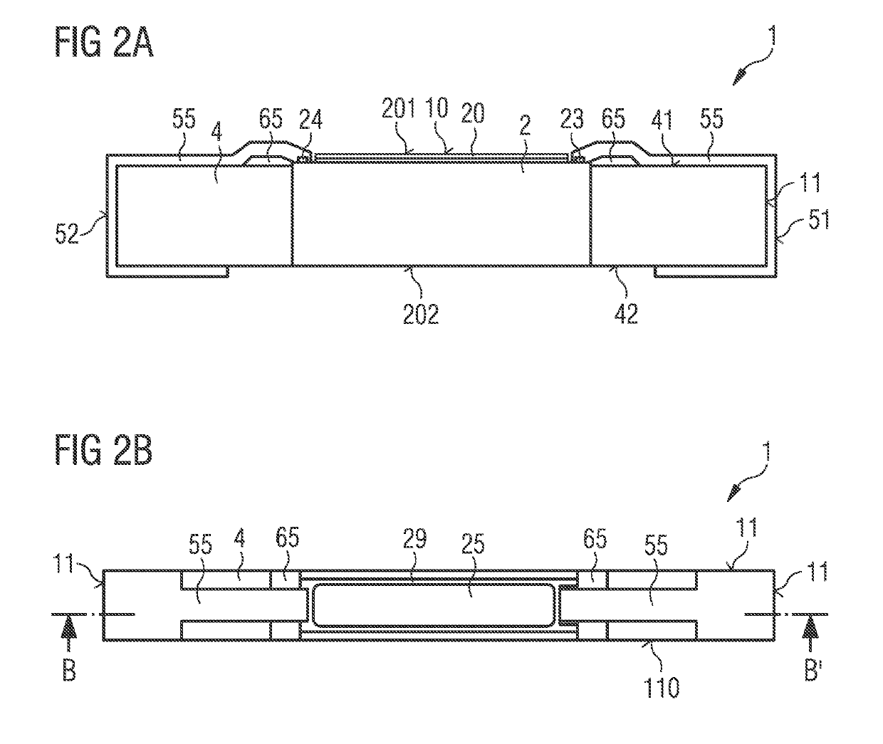
[0056]A first exemplary embodiment of a semiconductor device 1 is shown schematically in FIGS. 1A and 1B.

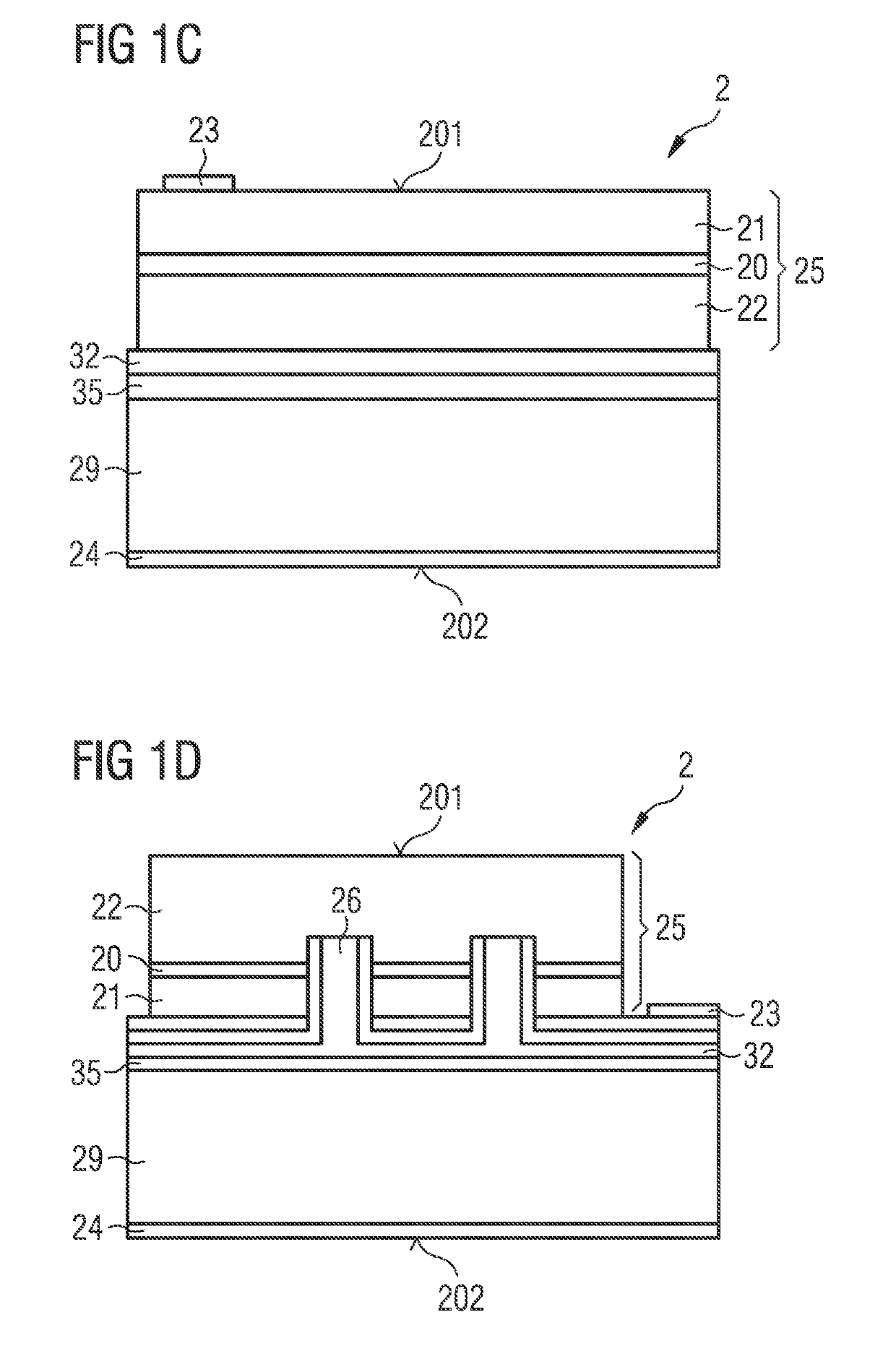
[0057]The semiconductor device 1 has a semiconductor chip 2 provided for generating radiation with a semiconductor layer sequence 25. The semiconductor layer sequence has an active region 20 provided for generating radiation. A radiation exit surface 10 of the semiconductor device runs parallel to the main extension plane of the active region. Details of the semiconductor chip 2 are explained in greater detail with reference to two exemplary embodiments in connection with FIGS. 1C and 1D.

[0058]Molded onto the semiconductor chip 2 is a molding 4. The molding 4 is used for the mechanical stabilization of the semiconductor chip and forms a housing for the semiconductor chip. The molding extends perpendicular to the radiation exit surface 10 between a rear side 42 of the molding lying opposite the radiation exit surface and a front side 41 of the molding. At the places at which the m...


PUM

PropertyMeasurementUnit
thicknessaaaaaaaaaa
reflectivityaaaaaaaaaa

Abstract

In an embodiment an optoelectronic semiconductor device includes a semiconductor chip having a semiconductor layer sequence with an active region, a radiation exit surface arranged parallel to the active region and a plurality of side faces arranged obliquely or perpendicular to the radiation exit surface. The device further includes a contact track electrically connecting the semiconductor chip to a contact surface configured to externally contact the semiconductor device, a molding and a rear side of the semiconductor chip remote from the radiation exit surface, the rear side being free of a material of the molding, wherein one of the side faces is configured as a mounting side face for fastening of the semiconductor device, and wherein the contact track partially runs on one of the side faces.

Description

[0001]This patent application is a national phase filing under section 371 of PCT / EP2015 / 078708, filed Dec. 4, 2015, which claims the priority of German patent application 10 2014 118 349.5, filed Dec. 10, 2014, each of which is incorporated herein by reference in its entirety.TECHNICAL FIELD[0002]The present application relates to an optoelectronic semiconductor device and a method for producing a plurality of optoelectronic semiconductor devices.BACKGROUND[0003]In handheld electronic devices, such as mobile telephones, for example, liquid crystal displays are often used, which are backlit by light-emitting diodes (LEDs) radiating laterally into light guides. In a reduction in the weight and depth of such devices, the light guides and LEDs must also be miniaturized further. In addition, it must be possible to produce the LEDs inexpensively. These requirements cannot be achieved easily with conventional designs.SUMMARY OF THE INVENTION[0004]One object is to specify an optoelectronic...

Claims


Application Information

Patent Timeline
Patent Type & Authority Patents(United States)
IPC IPC(8): H01L33/54H01L33/48H01L33/62H01L33/00H01L23/00H01L33/60H01L21/56
CPCH01L33/486H01L24/95H01L33/0093H01L33/54H01L33/60H01L33/62H01L21/568H01L2224/01H01L2224/24H01L2224/82H01L2924/0002H01L2924/181H01L2933/005H01L2933/0033H01L2224/06181H01L2224/96
Inventor SCHWARZ, THOMASSINGER, FRANK
Owner OSRAM OLED
Why Eureka
Try Eureka