Scheme of boosting adjustable ground level(s) of storage capacitor(s) of BJT pixel circuit(s) in pixel array circuit of image sensor apparatus

a technology of image sensor and storage capacitor, which is applied in the field of bipolar junction transistor pixel circuit, can solve the problems of unavoidably degrading image contrast, limited performance of conventional optical tracking system using pixel circuit having photo detector structure to sense the energy of incident light to capture image data, and poor optical tracking performance, so as to improve image quality, improve image contrast, and improve the effect of tracking performance of image sensor apparatus

Active Publication Date: 2022-03-22
PIXART IMAGING INC
View PDF10 Cites 0 Cited by
  • Summary
  • Abstract
  • Description
  • Claims
  • Application Information

AI Technical Summary

Benefits of technology

[0007]According to the embodiments, the image contrast of the BJT pixel units is significantly improved and thus the image quality is better. The tracking performance of the image sensor apparatus when applied to an optical tracking device / system is better compared to the conventional optical tracking device / system.

Problems solved by technology

Generally speaking, the performance of a conventional optical tracking system using a pixel circuit having a photo detector structure to sense the energy of the incident light to capture image data is limited by the environment light, the turn-on period of a shutter, or other factors associated with light source since the voltage of a storage capacitor of the pixel circuit easily becomes saturated in a situation of a higher light intensity when the storage capacitor is discharged.
The quality of image contrast will be unavoidably degraded due to the voltage saturation, and thus the performance of optical tracking is worse.

Method used


Image

  • Scheme of boosting adjustable ground level(s) of storage capacitor(s) of BJT pixel circuit(s) in pixel array circuit of image sensor apparatus
  • Scheme of boosting adjustable ground level(s) of storage capacitor(s) of BJT pixel circuit(s) in pixel array circuit of image sensor apparatus
  • Scheme of boosting adjustable ground level(s) of storage capacitor(s) of BJT pixel circuit(s) in pixel array circuit of image sensor apparatus

Examples


Embodiment Construction

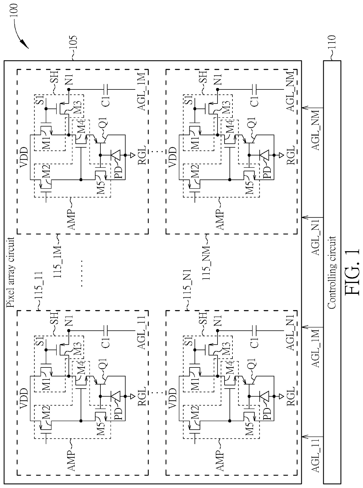
[0013]FIG. 1 is a diagram of an image sensor apparatus 100 according to an embodiment of the invention. The image sensor apparatus 100 is used for capturing image data of an illuminated navigation surface and comprises a pixel array circuit 105 and a controlling circuit 110. The pixel array circuit 105 comprises a plurality of bipolar junction transistor (BJT) pixel circuits 115_11, . . . , 115_1M, . . . , 115N1, . . . , and 115_NM, i.e. N×M BJT pixel circuits respectively corresponding to different pixel units spatially disposed on in a frame wherein the numbers of N and M are not limited.

[0014]Each BJT pixel circuit (e.g. 115_11, but not limited) at least comprises a photo detector PD such as a photodiode, a BJT transistor Q1, a shutter circuit SH, an amplifier circuit AMP, and a storage capacitor C1. For example, in this example, the shutter circuit SH comprises the transistors M1 and M3. The amplifier circuit AMP comprises transistors M2, M4, and M5. The storage capacitor C1 is ...


PUM


Abstract

A bipolar junction transistor (BJT) pixel circuit, including: a BJT transistor, having a base coupled to a photo detector, an emitter coupled to a shutter circuit, and a collector coupled to a reference ground level; the photo detector, having first end coupled to the base of BJT transistor and second end coupled to the reference ground level, for generating base current based on light intensity of light incident on the photo detector; the shutter circuit, coupled to the emitter of the BJT transistor, for controlling exposure time of the photo detector according to a shutter signal; and a storage capacitor, coupled between the shutter circuit and an adjustable ground level different from the reference ground level, for storing image data captured by the photo detector, wherein the adjustable ground level is boosted to be higher than the reference ground level for one or more times during the exposure time.

Description

BACKGROUND OF THE INVENTION1. Field of the Invention[0001]The invention relates to bipolar junction transistor pixel circuit, and more particularly to a bipolar junction transistor pixel circuit, a pixel array circuit, and an image sensor apparatus thereof.2. Description of the Prior Art[0002]Generally speaking, the performance of a conventional optical tracking system using a pixel circuit having a photo detector structure to sense the energy of the incident light to capture image data is limited by the environment light, the turn-on period of a shutter, or other factors associated with light source since the voltage of a storage capacitor of the pixel circuit easily becomes saturated in a situation of a higher light intensity when the storage capacitor is discharged. The quality of image contrast will be unavoidably degraded due to the voltage saturation, and thus the performance of optical tracking is worse.SUMMARY OF THE INVENTION[0003]Therefore one of the objectives of the inve...

Claims


Application Information

Patent Timeline
Patent Type & Authority Patents(United States)
IPC IPC(8): H01L27/146H04N5/235H04N5/3745
CPCH01L27/14681H04N5/2353H04N5/37452H04N23/54H04N23/75H04N23/73H04N25/771
Inventor LIM, WOOI KIP
Owner PIXART IMAGING INC
Why Eureka
Try Eureka