
Display panel and display device

a display panel and display device technology, applied in the field of touch display, can solve the problems of short circuit risk, low efficiency, and thinness at the edges of organic materials, so as to reduce the height difference of wirings, avoid inaccurate exposure and focus, and increase the thickness and height of blocking walls

Active Publication Date: 2022-05-10
WUHAN CHINA STAR OPTOELECTRONICS SEMICON DISPLAY TECH CO LTD
View PDF9 Cites 0 Cited by
  • Summary
  • Abstract
  • Description
  • Claims
  • Application Information

AI Technical Summary

Benefits of technology

This configuration results in a more accurate and reliable exposure process, reducing the risk of short circuits and ensuring a flat encapsulation layer, which enhances the manufacturing precision and reliability of OLED display panels.

Problems solved by technology

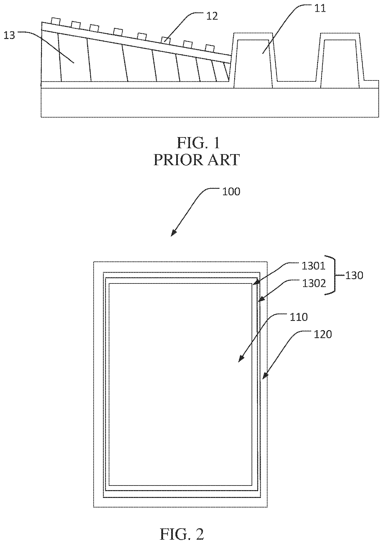
However, thickness at the edges of organics tends to become relatively thin.
However, due to a slope of the organic layer 13 produced by inkjet printing at the edges, DOT edge wirings have a problem of being out of focus during exposure and development.
As a result, the exposure of wiring 12 is not complete, and there is a risk of short circuit.

Method used


Image

  • Display panel and display device
  • Display panel and display device

Examples


Embodiment Construction

[0032]The following description of the embodiments with reference to the appended drawings is used for illustrating specific embodiments which may be used for carrying out the present disclosure. The directional terms described by the present disclosure, such as “upper”, “lower”, “front”, “back”, “left”, “right”, “inner”, “outer”, “side”, etc. are only directions by referring to the accompanying drawings. Names of elements mentioned in the present disclosure, such as first, second, etc., are only used to distinguish different components which can be better expressed. In figures, elements with similar structures are indicated with the same numbers.

[0033]Embodiments of the present disclosure will be described in detail herein with reference to the drawings. The disclosure may take many different forms, and the disclosure should not be construed as merely the specific embodiments set forth herein. The embodiments of the present disclosure are provided to explain a practical application...


PUM

PropertyMeasurementUnit
heightaaaaaaaaaa
heightaaaaaaaaaa
areaaaaaaaaaaa

Abstract

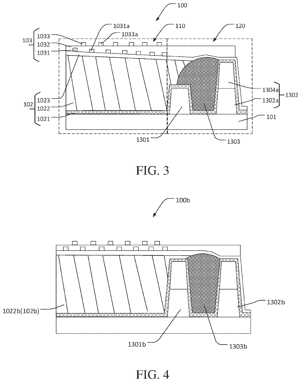
A display panel and a display device are provided and have a base substrate, a blocking wall, an encapsulation layer, and a touch capacitor layer. By forming a second-layer blocking wall and a first-layer blocking wall to form a second blocking wall, a height of the second blocking wall is increased. Further, a blocking block is disposed between the second blocking wall and the first blocking wall, thereby increasing a thickness and a height of the blocking wall. When inkjet printing an organic layer, a slope at edges of a display area is relatively smooth, which can make an entire encapsulation layer relatively flat, thereby reducing a height difference of wirings at the edges and avoiding a problem of inaccurate exposure and focus.

Description

RELATED APPLICATIONS[0001]This application is a National Phase of PCT Patent Application No. PCT / CN2019 / 123920 having International filing date of Dec. 9, 2019, which claims the benefit of priority of Chinese Patent Application No. 201910800332.0 filed on Aug. 28, 2019. The contents of the above applications are all incorporated by reference as if fully set forth herein in their entirety.FIELD AND BACKGROUND OF THE INVENTION[0002]The present disclosure relates to a technical field of touch display, and more particularly to a display panel and a display device.[0003]Organic light emitting diode (OLED) devices have advantages of simple structure, fast response speed, active light emission, and low power consumption. They have been widely used in display fields such as mobile phones, tablets, and televisions. Screen touch technology has also undergone iterative development. At present, external touch units are generally used, but in order to reduce an overall thickness of the display p...

Claims


Application Information

Patent Timeline
Patent Type & Authority Patents(United States)
IPC IPC(8): H01L51/52H01L27/32
CPCH01L51/5253H01L27/323H01L27/3276B32B37/06B32B37/08B32B37/10B32B17/10B32B17/10091B32B17/10972B32B17/1099B32B27/304H10K59/873H10K59/8722G06F3/03547H10K59/40H10K59/131H10K50/844
Inventor WANG, KUN
Owner WUHAN CHINA STAR OPTOELECTRONICS SEMICON DISPLAY TECH CO LTD
Learn More