Organic light-emitting diode display device and manufacturing method thereof

a technology of organic light-emitting diodes and display devices, which is applied in the field of display technologies, can solve the problems of oled display devices being particularly sensitive to water and oxygen, unstable excited state under ordinary environment, and prone to aging of metal electrodes and organic light-emitting materials, so as to prevent the organic layer and prevent the failure of oled display devices

Active Publication Date: 2022-05-17
WUHAN CHINA STAR OPTOELECTRONICS SEMICON DISPLAY TECH CO LTD
View PDF11 Cites 2 Cited by
  • Summary
  • Abstract
  • Description
  • Claims
  • Application Information

AI Technical Summary

Benefits of technology

[0017]The present invention relates to an organic light-emitting diode (OLED) display device and a method of manufacturing the same. In the present invention, the first retaining wall corresponding to the bending region is configured to include first retaining wall units spaced apart from each other, and a first buffer structure is formed in a gap provided between the first retaining wall units and is alternately connected to a left side and a right side of the first retaining wall units. The first retaining wall can achieve an effect of preventing the organic layer from overflowing during a printing process, Moreover, the stress generated during the bending of the OLED display device can be dispersed by the first buffer structure having elasticity. Therefore, excessive concentration of stress due to the special configuration of the retaining wall in the bending area, which causes the phenomenon of film layer detachment, can be prevented, thereby preventing the failure of the OLED display device.

Problems solved by technology

This excited state is unstable under an ordinary environment.
However, OLED devices are particularly sensitive to water and oxygen.
Metal electrodes and organic light-emitting material are prone to aging when in contact with water and oxygen.
A traditional encapsulating method is rigid encapsulation, but the devices cannot be bent after rigid encapsulation is performed.

Method used


Image

  • Organic light-emitting diode display device and manufacturing method thereof
  • Organic light-emitting diode display device and manufacturing method thereof
  • Organic light-emitting diode display device and manufacturing method thereof

Examples


embodiment 1

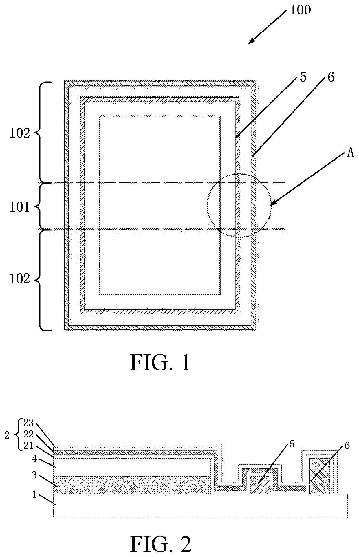
[0030]As shown in FIG. 1, an OLED display device 100 includes a bending region 101 and a non-bending region 102.

[0031]As shown in FIG. 2, the OLED display device 100 includes a substrate 1, a functional layer, and an encapsulation layer 2.

[0032]As shown in FIG. 1, FIG. 2, and FIG. 3, the functional layer is disposed on the substrate 1.

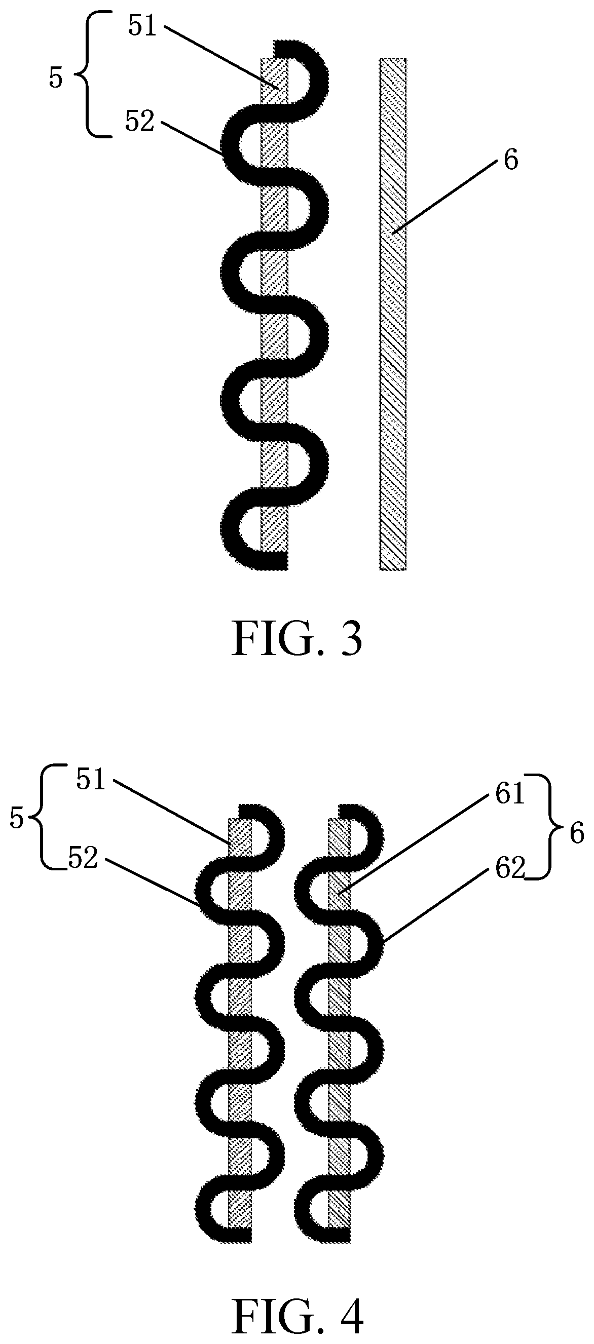
[0033]The functional layer includes a planarization layer 3 disposed on the substrate 1 and a pixel definition layer 4 disposed on the planarization layer 3. In fact, the functional layer further includes an active layer, a gate insulating layer, a gate layer, an interlayer insulating layer, a source-drain layer, and the like, and details are not described herein. The functional layer is further provided with a first retaining wall 5 and a second retaining wall 6 spaced from each other; wherein at least one section of the first retaining wall 5 includes first retaining wall units 51 spaced from each other and a first buffer structure 52 filled between ...

embodiment 2

[0043]As shown in FIG. 1, FIG. 3, and FIG. 4, the embodiment differs from embodiment 1 in that:

[0044]The second retaining wall 6 corresponding to the bending region 101 in the embodiment includes: second retaining wall units 61 and a second buffer structure 62. Wherein, the second retaining wall units 61 are spaced from each other; the second buffer structure 62 is disposed in a gap between the second retaining wall units 61 and is alternately connected to a left side and a right side of the second retaining wall units 61. In the embodiment, a shape of the second buffer structure 62 is similar to a wavy curve, and it can also be provided in a zigzag shape, a rectangular shape, or the like in an actual implementation. The shape of the second buffer structure 62 in the embodiment is preferably a wavy curve, which mainly disperses the stress generated during bending of the OLED display device 100 along the curve, which prevents the phenomenon of stress concentration, and finally preven...

embodiment 3

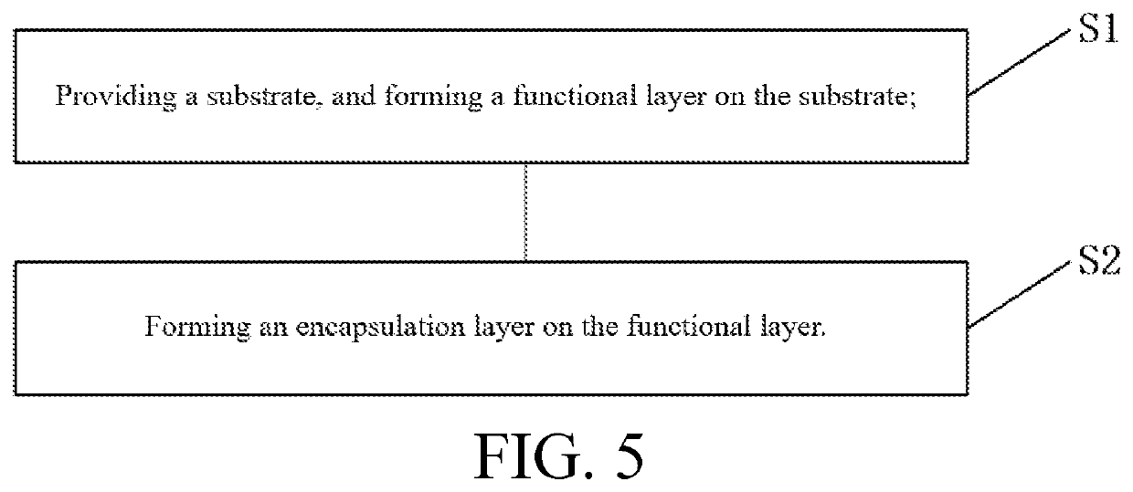
[0045]As shown in FIG. 5, the embodiment provides a method of manufacturing an organic light-emitting diode (OLED) display device 100 according to the present invention, which includes following steps: Step S1, providing a substrate 1, and forming a functional layer on the substrate 1; Step S2, forming an encapsulation layer 2 on the functional layer.

[0046]Step S1 includes forming a planarization layer 3 on the substrate 1 and forming a pixel definition layer 4 on the planarization layer 3.

[0047]Wherein, the first retaining wall 5 is formed by etching the planarization layer 3 at a position where the first retaining wall 5 is to be formed after the planarization layer 3 is formed and retaining the pixel definition layer 4 formed at the position in a subsequent process.

[0048]Wherein, the second retaining wall 6 is formed by retaining the planarization layer 3 at a position where the second retaining wall 6 is to be formed after the planarization layer 3 is formed and then stacking th...


PUM

PropertyMeasurementUnit
lengthaaaaaaaaaa
distanceaaaaaaaaaa
distanceaaaaaaaaaa

Abstract

The invention relates to an organic light-emitting diode (OLED) display device and a manufacturing method thereof. In the invention, a first retaining wall corresponding to a bending region is configured to include first retaining wall units spaced apart from each other, and a first buffer structure is formed in a gap provided between the first retaining wall units and is alternately connected to a left side and a right side of the first retaining wall units. This can prevent excessive stress concentration on the retaining wall in the bending region due to its special configuration, which causes a phenomenon of film layer detachment. Therefore, a failure of the OLED display device is prevented.

Description

FIELD OF INVENTION[0001]The present invention relates to the field of display technologies, and in particular, to an OLED display device and a manufacturing method thereof.BACKGROUND OF INVENTION[0002]Organic light-emitting diode (OLED) display devices are also known as organic electroluminescent display devices and organic light-emitting semiconductors. A working principle of OLED is: when electric power is supplied up to an appropriate voltage, an anode hole and a cathode charge will be combined in a light-emitting layer. Under action of Coulomb force, they will recombine to form excitons (electron-hole pairs) of an excited state. This excited state is unstable under an ordinary environment. Excitons in the excited state are recombined and transmit energy to a luminescent material, such that they transit from an energy level of a ground state to that of the excited state. Excited-state energy generates photons by a radiation relaxation process and releases light energy. Three prim...

Claims


Application Information

Patent Timeline
Patent Type & Authority Patents(United States)
IPC IPC(8): H01L51/52H01L51/56
CPCH01L51/5253H01L51/56H01L2251/5338H10K59/122H10K50/8428H10K50/844H10K59/124H10K2102/311H10K71/00
Inventor WANG, KUN
Owner WUHAN CHINA STAR OPTOELECTRONICS SEMICON DISPLAY TECH CO LTD
Why Eureka
Try Eureka