
Solid-state imaging element, imaging apparatus, and method for controlling solid-state imaging element

a technology of solid-state imaging and imaging elements, which is applied in the direction of color television details, television system details, television system control, etc., can solve the problems of deteriorating the signal-noise ratio of the pixel signal, ktc noise is generated, and 1/f noise in the small-sized pixel amplifier transistor, so as to increase the read speed and reduce the noise component

Active Publication Date: 2022-05-31
SONY SEMICON SOLUTIONS CORP
View PDF4 Cites 0 Cited by
  • Summary
  • Abstract
  • Description
  • Claims
  • Application Information

AI Technical Summary

Benefits of technology

[0016]According to the present technology, an excellent effect of increasing the read speed while reducing the noise component can be obtained. Note that effects described herein are not necessarily limited, but may also be any of those described in the present disclosure.

Problems solved by technology

Here, in the process of sampling and holding the pixel signal by the sample-hold circuit, kTC noise is generated due to the on / off of a switch in the circuit.
Furthermore, in the pixel circuit preceding the sample-hold circuit, 1 / f noise occurs in a small-sized pixel amplifier transistor.
These noise components deteriorate the signal-noise (SN) ratio of the pixel signal.

Method used


Image

  • Solid-state imaging element, imaging apparatus, and method for controlling solid-state imaging element
  • Solid-state imaging element, imaging apparatus, and method for controlling solid-state imaging element
  • Solid-state imaging element, imaging apparatus, and method for controlling solid-state imaging element

Examples


first embodiment

1. First Embodiment

[0045][Configuration Example of Imaging Apparatus]

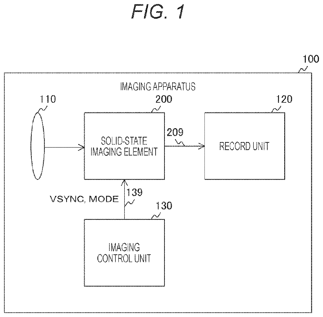
[0046]FIG. 1 is a block diagram illustrating a configuration example of an imaging apparatus 100 according to the first embodiment of the present technology. The imaging apparatus 100 is an apparatus that captures image data, and includes an imaging lens 110, a solid-state imaging element 200, a record unit 120, and an imaging control unit 130. As the imaging apparatus 100, a digital camera such as an IoT camera or an electronic apparatus (e.g., a smartphone or a personal computer) having an imaging function is assumed.

[0047]The solid-state imaging element 200 captures image data under the control of the imaging control unit 130. The solid-state imaging element 200 supplies the image data to the record unit 120 via a signal line 209.

[0048]The imaging lens 110 collects light and guides the collected light to the solid-state imaging element 200. The imaging control unit 130 causes the solid-state imaging element 200 ...

second embodiment

2. Second Embodiment

[0131]In the above-described first embodiment, in the decimation mode, the timing control circuit 240 connects the plurality of capacitances 278 to the signal line in parallel to reduce the noise component. However, while the noise component can be reduced, rows and columns are decimated, resulting in a reduction in resolution. The timing control circuit 240 according to the second embodiment differs from that of the first embodiment, in that the plurality of capacitances 278 is connected in parallel to the signal line without decimation.

[0132]FIG. 13 is a timing chart illustrating an example of an operation of the solid-state imaging element when a high image quality mode is set according to the second embodiment of the present technology. In the second embodiment, one of the normal mode and the high image quality mode is set. Here, the high image quality mode is a mode in which a noise component is reduced by connecting the plurality of capacitances 278 in para...

third embodiment

3. Third Embodiment

[0142]In the above-described first embodiment, the solid-state imaging element 200 samples the pixel signals only once. However, with only one sampling, there is a possibility that a noise component generated in the pixel cannot be removed from the pixel signal. The solid-state imaging element 200 according to the third embodiment is different from that of the first embodiment in that correlated double sampling (CDS) processing is performed on pixel signals.

[0143]FIG. 14 is a block diagram illustrating a configuration example of the sample-hold block 260 according to the third embodiment of the present technology. The sample-hold block 260 of the third embodiment differs from that of the first embodiment in that a pair of sample-hold circuits 270 is provided with respect to each column. For example, when the number of columns is M, 2×M sample-hold circuits 270 are arranged. The switch 261 is also doubled in accordance with the doubling of the number of sample-hold...


PUM


Abstract

To improve an SN ratio in a solid-state imaging element provided with a capacitance for reducing a noise component.A first capacitance connection circuit connects one end of a first capacitance to a first signal line in a case where a first pixel signal is transmitted via the first signal line. A second capacitance connection circuit connects one end of a second capacitance to a second signal line in a case where a second pixel signal is transmitted via the second signal line. An intercapacitance connection circuit connects one end of each of the first capacitance and the second capacitance in a case where one of the first pixel signal and the second pixel signal is transmitted, and disconnects one end of each of the first capacitance and the second capacitance in a case where both the first pixel signal and the second pixel signal are transmitted.

Description

TECHNICAL FIELD[0001]The present technology relates to a solid-state imaging element, an imaging apparatus, and a method for controlling a solid-state imaging element. More specifically, the present technology relates to a solid-state imaging element in which an analog-to-digital converter is arranged for each column, an imaging apparatus, and a method for controlling the solid-state imaging element.BACKGROUND ART[0002]Conventionally, in a solid-state imaging element, a column analog-to-digital converter (ADC) system in which an ADC is arranged for each column of pixels has been widely used. In this column ADC system, a sample-hold circuit that samples a pixel signal and holds the signal over a conversion period is often arranged at a stage preceding the ADC for each column. Here, in the process of sampling and holding the pixel signal by the sample-hold circuit, kTC noise is generated due to the on / off of a switch in the circuit. Furthermore, in the pixel circuit preceding the samp...

Claims


Application Information

Patent Timeline
Patent Type & Authority Patents(United States)
IPC IPC(8): H04N5/378H04N5/3745
CPCH04N5/378H04N5/37457H04N25/616H04N25/65H04N25/75H04N25/778
Inventor LUONG, HUNG
Owner SONY SEMICON SOLUTIONS CORP
Learn More