AI-driven self adapting microelectronic circuits

a microelectronic circuit and self-adaptive technology, applied in the field of artificial intelligence, can solve the problems of unnecessarily large, hotter, more complex, less optimal microelectronic circuits that fail, waste of power and performance, and waste of spa

Active Publication Date: 2022-08-16
ANALOG INTELLIGENT DESIGN INC
View PDF0 Cites 1 Cited by
  • Summary
  • Abstract
  • Description
  • Claims
  • Application Information

AI Technical Summary

Benefits of technology

[0011]Since these additional circuitries take up some area, they can be applied to several microelectronic circuit blocks on the same chip to amortize the overall impact. Their additional power consumption can also be kept low by keeping them idle or in sleep mode until only when changes are required. In many implementations, there is already one or more CPUs available to perform other system functions. The self-adaptation function by the AI engine is just added to the main functions of the CPU.
[0016]At the hardware level, the design of the microelectronic circuits involves the implementation of the desired circuit function (“functional section”) as well as that of the additional circuits or functions (“adaptation section”) required to bring its operation or characteristics back to the original specifications. This is where a fundamental methodology change occurs. In the current and prior art, the designer must come up with various complex circuits or design tricks that ensure functionality over a wide spectrum of usage and environmental conditions. His focus is on extensively simulate the circuits and verify that they work. This methodology increases the complexity, area, power, and the risk of failure of the circuits due to unforeseen behavior, inadequate simulation coverage, etc. With the current methodology, the base circuit design is simpler but is capable of changing itself to negate all or part of the effects on its performance characteristics caused by changes in the usage and environmental conditions and achieve a very tight set of specifications over the wide range of conditions.
[0017]With the new methodology in this description, the designer creates the base circuit then focuses on the circuit changes to be activated under the various usage and environmental conditions. Such circuit changes can range from simple device size changes, additional gates, data bits, or even additional functions like amplifier stages, current sources, etc. Meanwhile, the “base” circuit can be very simple. The complexity of the design changes from that of the base circuit to that of add-on adaptation circuits that realize the desired changes to the base circuit. To simplify the task, libraries of add-ons or libraries of adaptable base circuits can be created.
[0019]It is an advantage of this description to be able to produce microelectronic circuits that can change themselves according to the usage or environmental conditions to negate all or part of their effects on the circuit performance characteristics or maintain their originally specified functionality.
[0020]It is another advantage of this description to be able to produce microelectronic circuits that can learn from the usage and environmental conditions and change themselves to provide certain new functionality or characteristics.
[0021]It is yet another advantage of this description is the achievement of much tighter specifications of the circuits over the environmental and usage conditions compared to the current methodology, increasing overall performance of the circuit and the system using it.

Problems solved by technology

Such “design-for-worse-case” methodology has been ongoing for decades, creating unnecessarily larger, hotter, more complex, less optimal microelectronic circuits that fail as soon as they encounter conditions outside of the specified ranges.
The wasted area, power and performance is also unnecessary since most circuits operate in or near nominal environmental conditions.

Method used


Image

  • AI-driven self adapting microelectronic circuits
  • AI-driven self adapting microelectronic circuits
  • AI-driven self adapting microelectronic circuits

Examples


Embodiment Construction

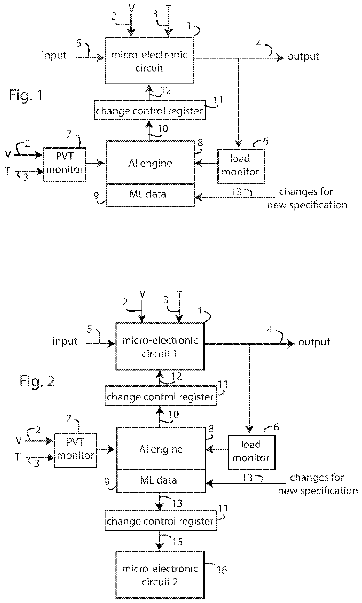
[0062]In general, the present description is a method based on artificial intelligence to implement a wide range of microelectronic circuits that can adapt by themselves to the usage conditions (e.g. loading changes), manufacturing variances or defects (e.g. process variations, device parameter mismatches, device model inaccuracies or changes, etc.) as well as environmental conditions (e.g. voltage, temperature) in order to negate all or part of their effects on the circuit performance characteristics and achieve a very tight set of specifications over the wide range of conditions.

[0063]The system includes (see FIG. 1) a Microelectronic Circuit 1, a Load Monitor 6, a PVT monitor 7, an AI engine 8 with stored machine learning data 9 and a Change Control Register 11. In some implementations, the Load Monitor is not present.

[0064]The Microelectronic Circuit 1 is designed to function and provides certain outputs 4 within a certain range of the usage conditions (e.g. loading, interferenc...


PUM


Abstract

The present description relates to a method based on artificial intelligence to implement a wide range of microelectronic circuits that can adapt by themselves to the usage conditions (e.g. loading changes), manufacturing variances or defects (e.g. process variations, device parameter mismatches, device model inaccuracies or changes, etc.), as well as environmental conditions (e.g. voltage, temperature, interference) in order to negate all or part of their effects on the circuit performance characteristics and achieve a very tight set of specifications over the wide range of conditions. Each microelectronic circuit is represented by a neural network model whose behavior is a function of the actual input signals, the usage and environmental conditions. An attached AI engine will infer from the model, the input signals, the usage conditions and the environmental conditions and create the adaptive changes required to modify the microelectronic circuit's behavior to negate all or part of their effects on the circuit performance characteristics and to achieve a very tight set of specifications.

Description

BACKGROUNDField of the Invention[0001]The present invention relates to a method based on artificial intelligence to implement a wide range of microelectronic circuits that can adapt by themselves to the usage conditions (e.g. loading changes), manufacturing variances or defects (e.g. process variations, device parameter mismatches, device model inaccuracies or changes, etc.) as well as environmental conditions (e.g. voltage, temperature) in order to negate all or part of their effects on the performance characteristics circuit block. In accordance with the present description, a machine learning model is used to represent the behavior of the microelectronic circuits in response to changes in the conditions on their operation. Built from machine learning data derived from simulation, the machine learning model will infer appropriate internal changes to the circuit components, e.g. sizes, functionality, connections, etc., in order to negate all or part of the effects on the circuit pe...

Claims


Application Information

Patent Timeline
Patent Type & Authority Patents(United States)
IPC IPC(8): G06F30/367G06N3/08
CPCG06F30/367G06N3/08G06N3/063
Inventor LE, KHANH MDE, KOUSHIKAMURU, DEEPTHIABBAS, ZIA
Owner ANALOG INTELLIGENT DESIGN INC
Why Eureka
Try Eureka