Display apparatus

Active Publication Date: 2022-11-08
PLAYNITRIDE DISPLAY CO LTD
View PDF18 Cites 2 Cited by
  • Summary
  • Abstract
  • Description
  • Claims
  • Application Information

AI Technical Summary

Benefits of technology

[0005]The disclosure provides a display apparatus capable of providing large-scale display with favorable display quality and production yield.
[0020]To sum up, in the display apparatus by an embodiment of the disclosure, the light emitting display units are provided with the driving circuit layers. In this way, the margin of circuit design of the display apparatus is increased, and the bonding region of the light emitting display units for electrically bonding the circuit boards may also be effectively reduced. As such, the light emitting display units located around the circuit boards may overlap the board edges of the circuit boards. Accordingly, seamless splicing of the light emitting display units on the circuit boards may be accomplished, and display quality of the large-sized display apparatus is thereby improved. From another perspective, through the electrical bonding of the light emitting display units and the circuit boards, difficulty of repairing of the display apparatus may be lowered. In other words, probability of the display apparatus being scrapped due to failure of transposition (transferring and positioning) of part of the light emitting devices may be effectively reduced, and the production yield of the display apparatus is therefore improved.

Problems solved by technology

Therefore, how to solve the foregoing problem is an important issue in the industry in the development of the splicing display technology.
From another perspective, through the electrical bonding of the light emitting display units and the circuit boards, difficulty of repairing of the display apparatus may be lowered.

Method used


Image

  • Display apparatus
  • Display apparatus
  • Display apparatus

Examples


first embodiment

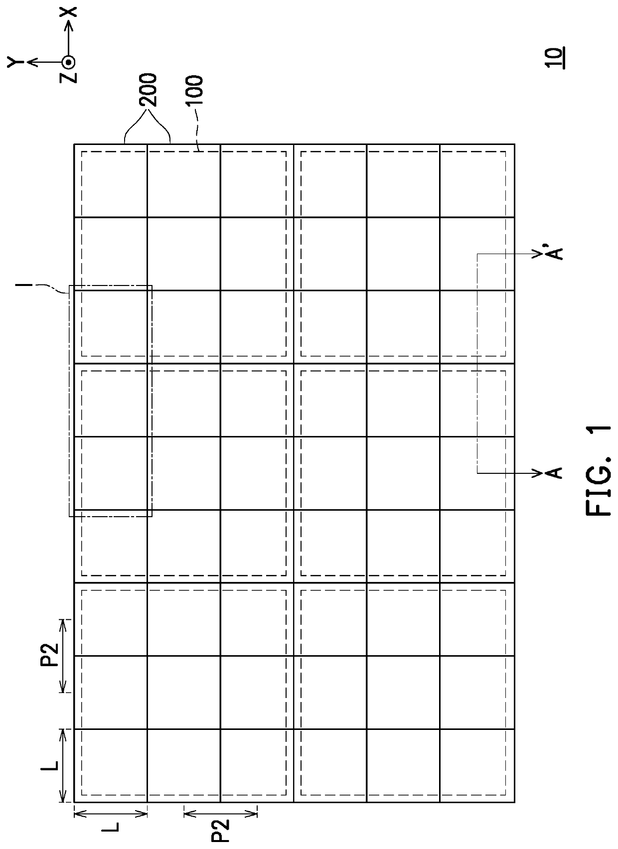
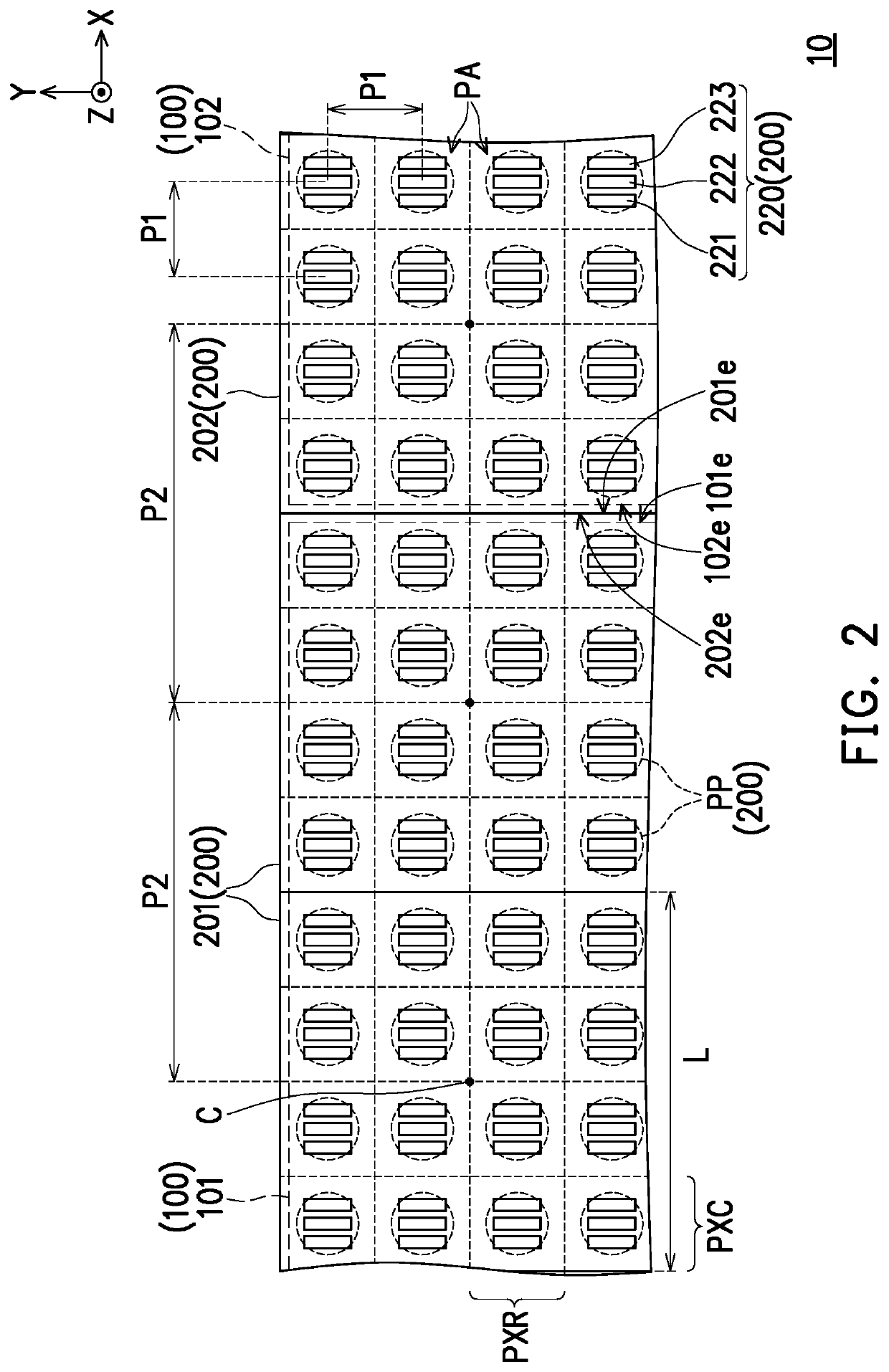
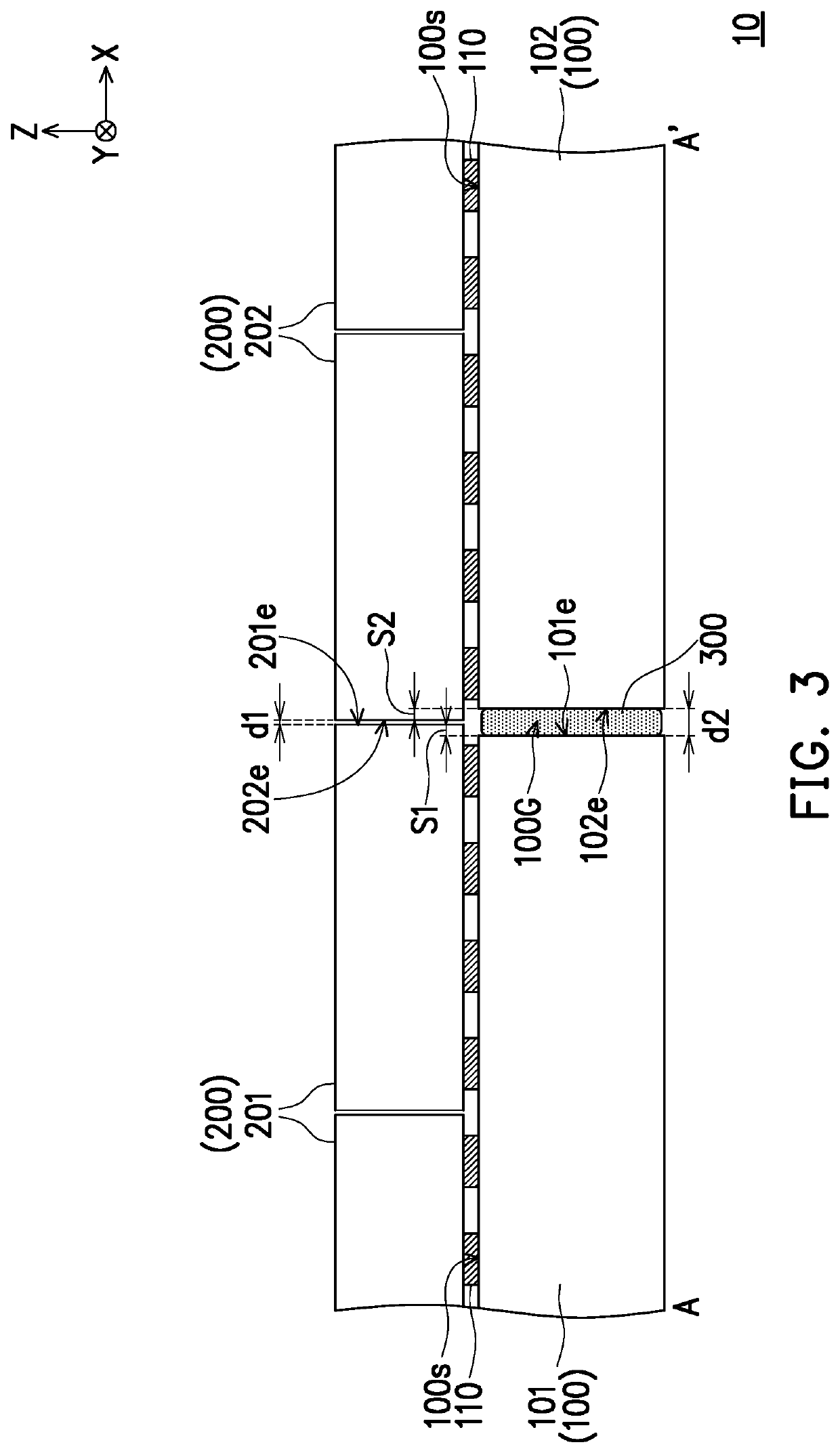
[0034]FIG. 1 is a front schematic view of a display apparatus according to the disclosure. FIG. 2 is an enlarged schematic view of a local region of the display apparatus of FIG. 1. FIG. 2 corresponds to a region I of FIG. 1. FIG. 3 is a cross-sectional schematic view of the display apparatus of FIG. 1. FIG. 3 corresponds to a cross-sectional line A-A′ of FIG. 1. FIG. 4 is a cross-sectional schematic view of light emitting display units of FIG. 1. FIG. 5 is a front schematic view of a display apparatus according to another embodiment of the disclosure. For clarity and description, only a light emitting device 220 and a pad structure PP of FIG. 4 are illustrated in a light emitting display unit 200 of FIG. 2, and illustration of detailed members of the light emitting display unit 200 of FIG. 4 is omitted in FIG. 3.

[0035]With reference to FIG. 1 to FIG. 4, a display apparatus 10 includes a plurality of circuit boards 100 and a plurality of light emitting display units 200. These light...

second embodiment

[0059]FIG. 6 is a cross-sectional schematic view of a display apparatus according to the disclosure. With reference to FIG. 6, a difference between a display apparatus 10B of this embodiment and the display apparatus 10 of FIG. 3 is that: light emitting display units 200′ of the display apparatus 10B are required to be processed through a cutting process before being transposed to the circuit boards 100. That is, in this embodiment, a clearly visible gap G is provided between any adjacent two of the light emitting display units 200′ located on the same circuit board 100. This gap G may act as a buffering space of the light emitting display units 200′ for volume expansion caused by heating during a transposition and bonding process, and a transfer yield of the light emitting display units 200′ may thus be increased. Note that a spacing S3 of the gap G between any adjacent two light emitting display units 201′ (or light emitting display units 202′) in an arrangement direction (e.g., d...

third embodiment

[0062]FIG. 7 is a front schematic view of a display apparatus according to the disclosure. FIG. 8 is an enlarged schematic view of a local region of the display apparatus of FIG. 7. FIG. 8 corresponds to a region II of FIG. 7. FIG. 9 is a cross-sectional schematic view of the display apparatus of FIG. 7. FIG. 9 corresponds to a cross-sectional line B-B′ of FIG. 7.

[0063]With reference to FIG. 7 to FIG. 9, a difference between a display apparatus 20 of this embodiment and the display apparatus 10 of FIG. 1 is that: the display apparatus 20 provides a different structure and a different shape. To be specific, in the visual direction (e.g., direction Z), an outer contour of the display apparatus 20 is non-rectangular, and the non-rectangular contour is formed by splicing of two circuit boards of different sizes. In this embodiment, the display apparatus 20 includes a plurality of circuit boards 100A and a plurality of circuit boards 100B, and sizes of the circuit boards 100A are greater...


PUM

PropertyMeasurementUnit
thicknessaaaaaaaaaa
lengthaaaaaaaaaa
distance d1aaaaaaaaaa

Abstract

A display apparatus includes a first circuit board and a plurality of first light emitting display units. The first circuit board has a first surface and a first board edge connected to the first surface. The first light emitting display units are disposed on the first surface. Each of the first light emitting display units has a plurality of first pixel areas and includes a first driving circuit layer electrically bonded to the first circuit board and a plurality of first light emitting devices. The first light emitting devices are disposed on one side of the first driving circuit layer away from the first circuit board and are electrically bonded to the first driving circuit layer. At least one of the first light emitting display units has a first side edge parallel to the first board edge. The first board edge is drawn back from the first side edge.

Description

CROSS-REFERENCE TO RELATED APPLICATION[0001]This application claims the priority benefits of U.S. provisional application Ser. No. 63 / 069,693, filed on Aug. 24, 2020, and Taiwan application serial no. 109145631, filed on Dec. 23, 2020. The entirety of each of the above-mentioned patent applications is hereby incorporated by reference herein.BACKGROUNDTechnical Field[0002]The disclosure relates to a display technology, and in particular, relates to a spliced display apparatus.Description of Related Art[0003]As applications of display apparatuses gradually diversified, the use of large display boards for displaying public messages or advertisements in major exhibition halls or department stores has become increasingly popular. In order to reduce the costs of installation and maintenance of these large display boards, adoption of a spliced display apparatus formed by splicing of multiple display panels has become one of the common mounting methods for these large display boards. Genera...

Claims


Application Information

Patent Timeline
Patent Type & Authority Patents(United States)
IPC IPC(8): G09F9/302G09F9/33H01L33/48H01L33/62H01L27/15
CPCG09F9/3026G09F9/33H01L27/156H01L33/486H01L33/62H01L25/167H01L25/0753
Inventor TSENG, CHUN-MINGLIN, WEI-PINGSU, PO-JENSHEU, GWO-JIUN
Owner PLAYNITRIDE DISPLAY CO LTD
Why Eureka
Try Eureka