Array substrate for use in LCD device

a technology of array substrate and lcd device, which is applied in the direction of semiconductor devices, instruments, optics, etc., can solve the problems of serious inferiority of lcd device, serious problems with alien substance and defect, and decrease of manufacturing yield of lcd devi

Inactive Publication Date: 2001-08-16
LG DISPLAY CO LTD
View PDF0 Cites 33 Cited by
  • Summary
  • Abstract
  • Description
  • Claims
  • Application Information

AI Technical Summary

Problems solved by technology

However, pure Aluminum is weak in acidity and may result in line defects by a formation of a hillock during a high temperature process, so Aluminum alloy and multi-layered Aluminum are used.
Such alien substance and defect have become serious problems in accordance with the conventional art due to the impossibility of the repair.
Therefore, the gate and data lines 22 and 24 come into a line defect causing the serious inferiority in the LCD device.
Therefore, this also comes into the line defect causing the decrease of manufacturing yields of the LCD device.

Method used


Image

  • Array substrate for use in LCD device
  • Array substrate for use in LCD device
  • Array substrate for use in LCD device

Examples


first embodiment

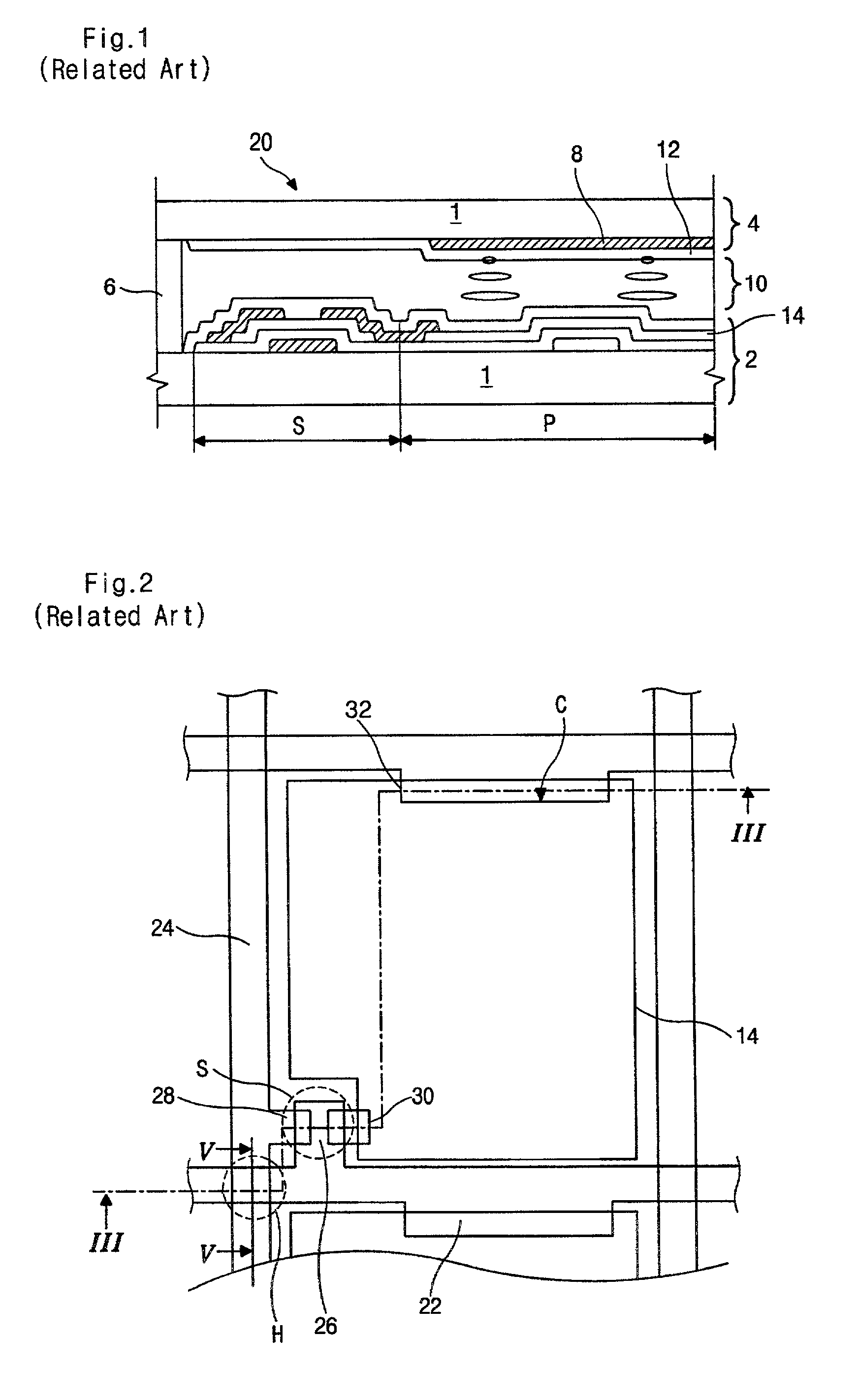
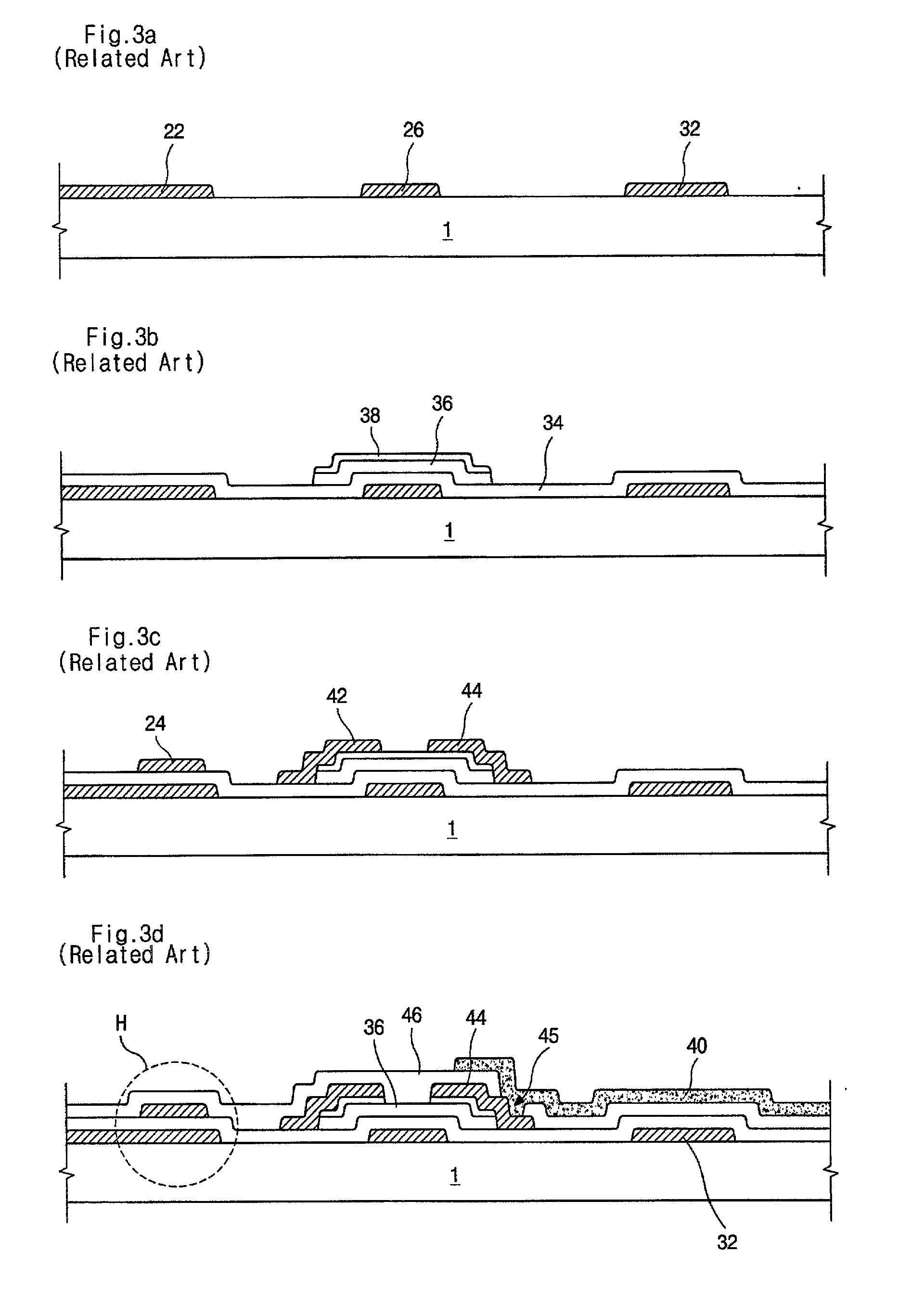
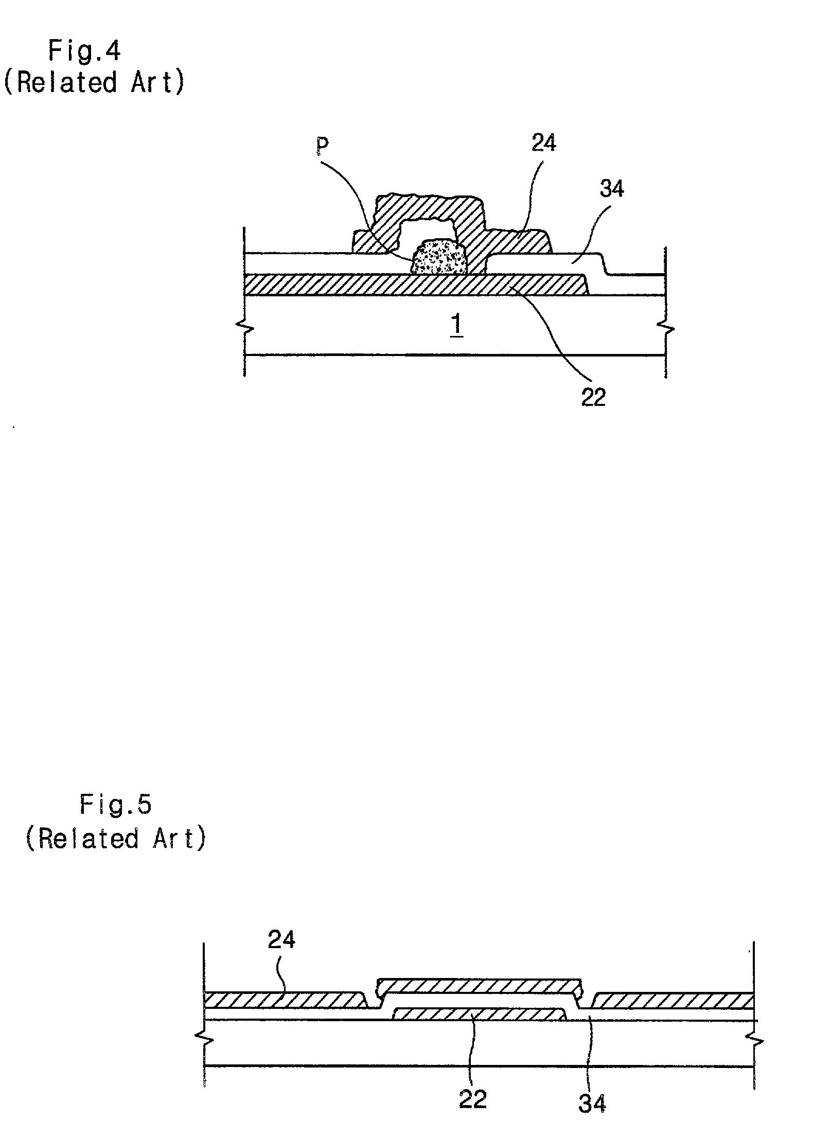
[0044] FIG. 9 illustrates a method of repairing the short of the gate and data lines according to the present invention. The data line 110 formed on the gate insulation layer 124 with the alien substance "P" is electrically short-circuited to the gate line 100. Hence, both sides of the short-circuited portion of the data line 110 is cut by a laser or other equipments having a high energy density. Thus, the data line 110 is divided into first and second data lines 110a and 110b, each positioned opposing sides of the cutting portions "C". Therefore, by cutting the data line 110, the first and second data lines 110a and 110b are electrically independent, and then the first and second repair lines 118 and 122 are used for connecting the first and second data lines 110a and 110b.

[0045] As shown in FIG. 9, to repair the data line 110, the overlapped portions "W" of the second repair line 122, each corresponding to the second data line 110b and the first repair line 118, are welded by the ...

second embodiment

[0052] As mentioned above, the present invention suggests the repair line which is independent of the pixel electrode and prevents the short-circuit and the open-circuit at the cross point of the gate and data lines. When the short-circuit or the open-circuit occurs, the cutting and welding process can repair them using the repair line and a laser.

[0053] According to the first and second embodiment, the repair line is formed while forming the pixel electrode so that additional process steps are not required. Accordingly, without increase of the manufacturing cost, the repairing can be achieved.


PUM

PropertyMeasurementUnit
optical anisotropyaaaaaaaaaa
orientational orderaaaaaaaaaa
electric fieldaaaaaaaaaa

Abstract

A TFT array substrate for use in LCD device includes at least one repair line to repair the line defects. The repair line(s) is formed when forming the pixel electrode so that additional process steps are not required. Accordingly, the productivity can increase. Moreover, either the short-circuit or the open-circuit can be repaired due to the the repair line(s). Thus, in the present invention, a TFT array substrate, including: a substrate; a gate line formed on the substrate, arranged in a transverse direction and having a gate electrode; a data line insulated against the gate line by a first insulation layer, arranged in a longitudinal direction perpendicular to the gate line, having a source electrode near the cross point of the gate and data lines, and having first and second data lines which are defined by a cross point of the gate and data lines; a drain electrode space apart from the source electrode over the gate electrode; a pixel electrode connecting to the drain electrode; and a repair line(s) insulated against the data and gate lines by insulation layers and overlapping the gate and data lines, the repair line(s) overlapping a free end of the other repair line and the gate line.

Description

CROSS REFERENCE[0001] This application claims the benefit of Korean Patent Application No. 1999-58750, filed on Dec. 17, 1999, which is hereby incorporated by reference.[0002] 1. Field of the Invention[0003] The present invention relates to a liquid crystal display (LCD) device, and more particularly, to an array substrate of the LCD device having thin film transistors.[0004] 2. Description of Related Art[0005] In general, a liquid crystal display (LCD) device displays an image using a plurality of pixels. The LCD device having a thin film transistor (TFT) as a switching element is typically called a thin film transistor liquid crystal display (TFT-LCD) device.[0006] A typical liquid crystal display device uses optical anisotropy and polarization properties of liquid crystal molecules. The liquid crystal molecules have a definite orientational order in arrangement resulting from their thin and long shapes. The arrangement direction of the liquid crystal molecules can be controlled b...

Claims


Application Information

Patent Timeline
Patent Type & Authority Applications(United States)
IPC IPC(8): G02F1/136G02F1/1362G02F1/1368
CPCG02F1/1368G02F2001/136272G02F1/136272G02F1/136
Inventor AHN, BYUNG-CHULLEE, JAE-GUJUNG, YU-HO
Owner LG DISPLAY CO LTD
Why Eureka
Try Eureka