Substrate for semiconductor device and semiconductor device fabrication using the same

Inactive Publication Date: 2001-09-20
NEC ELECTRONICS CORP
View PDF0 Cites 6 Cited by
  • Summary
  • Abstract
  • Description
  • Claims
  • Application Information

AI Technical Summary

Problems solved by technology

If so, when the electric charge on the substrate 110 is discharged instantaneously, the charge will pass through the semiconductor element or IC chip mounted on the substrate 110, resulting in the danger that the element or chip is broken electrostatically.
First, with the improved technique, there is the need to form the short-circuiting line or pattern in such a way that part of the terminals are selectively short-circuited according to necessity. Therefore, when the improved technique is applied to the substrates of the type designed for semiconductor devices with the BGA or LGA package, it is often difficult to provide a space or room for the short-circuiting line or pattern on the substrate. This is because the wiring lines are arranged on the substrate at a considerably high density. As a results it is seen that the improved technique is difficult to be applied to the substrates for the BGA- or LGA-packaged semiconductor devices.
Second, since the terminals on the printed wiring board are short-circuited with the short-circuiting line or pattern, desired electrical tests for inspection are unable to be carried out just after a semiconductor element or IC chip is mounted.
Third, even if the terminals on the board are short-circuited with the short-circuiting line or pattern, the board itself is kept in an electrically floating state. Thus, it is difficult to release the electric charge from the terminals. This means that it is difficult or unable to surely prevent the semiconductor element or IC chip from being broken or damaged electrostatically.
Fourth, the improved technique necessitates a dedicated process of eliminating the short-circuiting line or pattern. Thus, the total step number of the fabrication process sequence increases.

Method used


Image

  • Substrate for semiconductor device and semiconductor device fabrication using the same
  • Substrate for semiconductor device and semiconductor device fabrication using the same
  • Substrate for semiconductor device and semiconductor device fabrication using the same

Examples


first embodiment

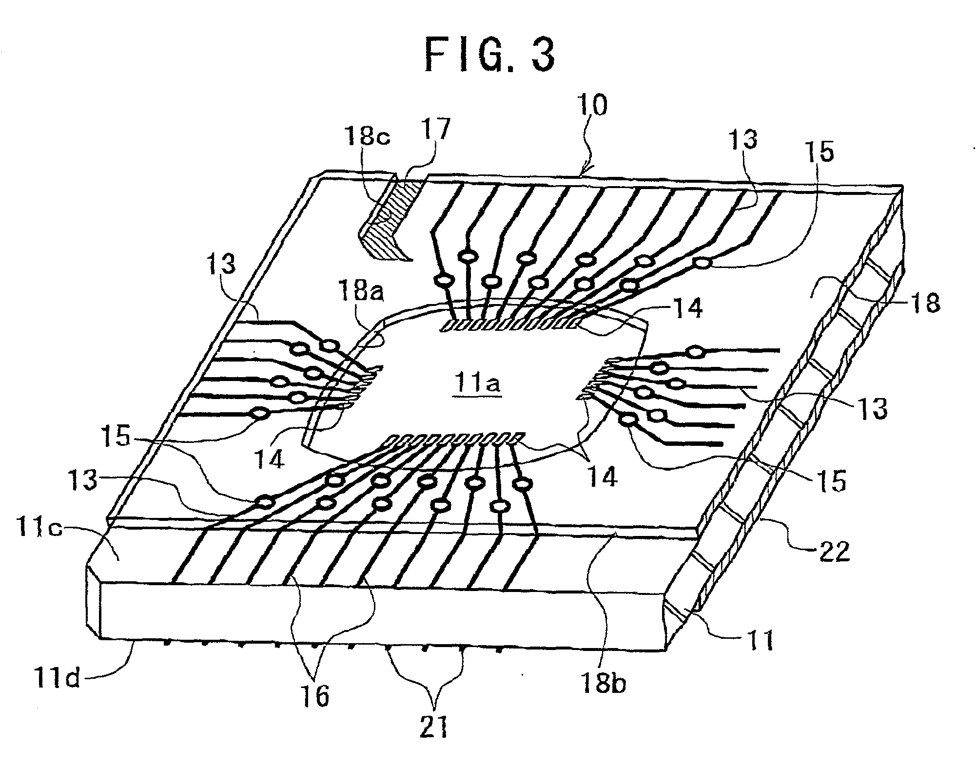
[0103] A substrate for a semiconductor device according to the invention is shown in FIGS. 3 to 6.

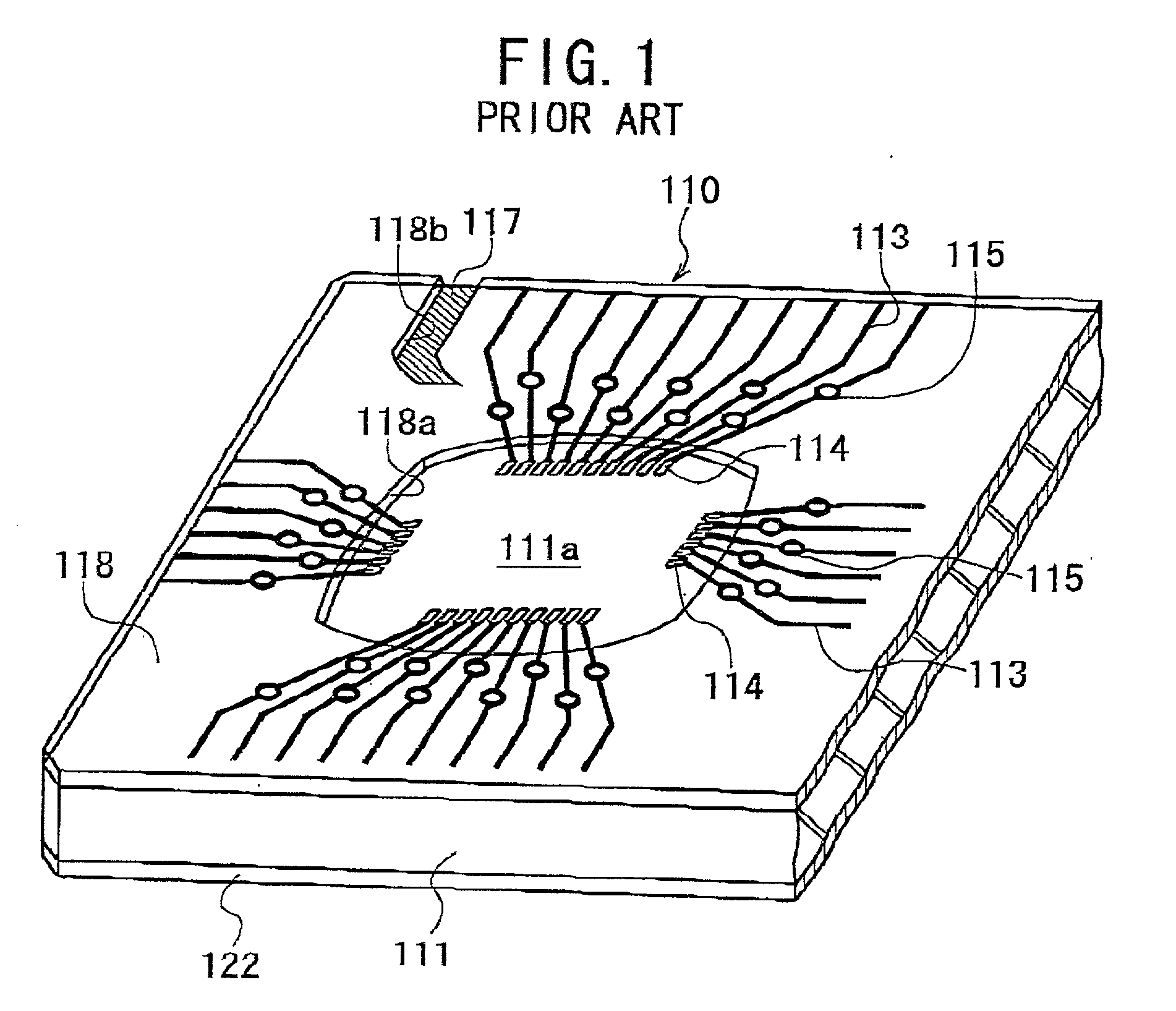
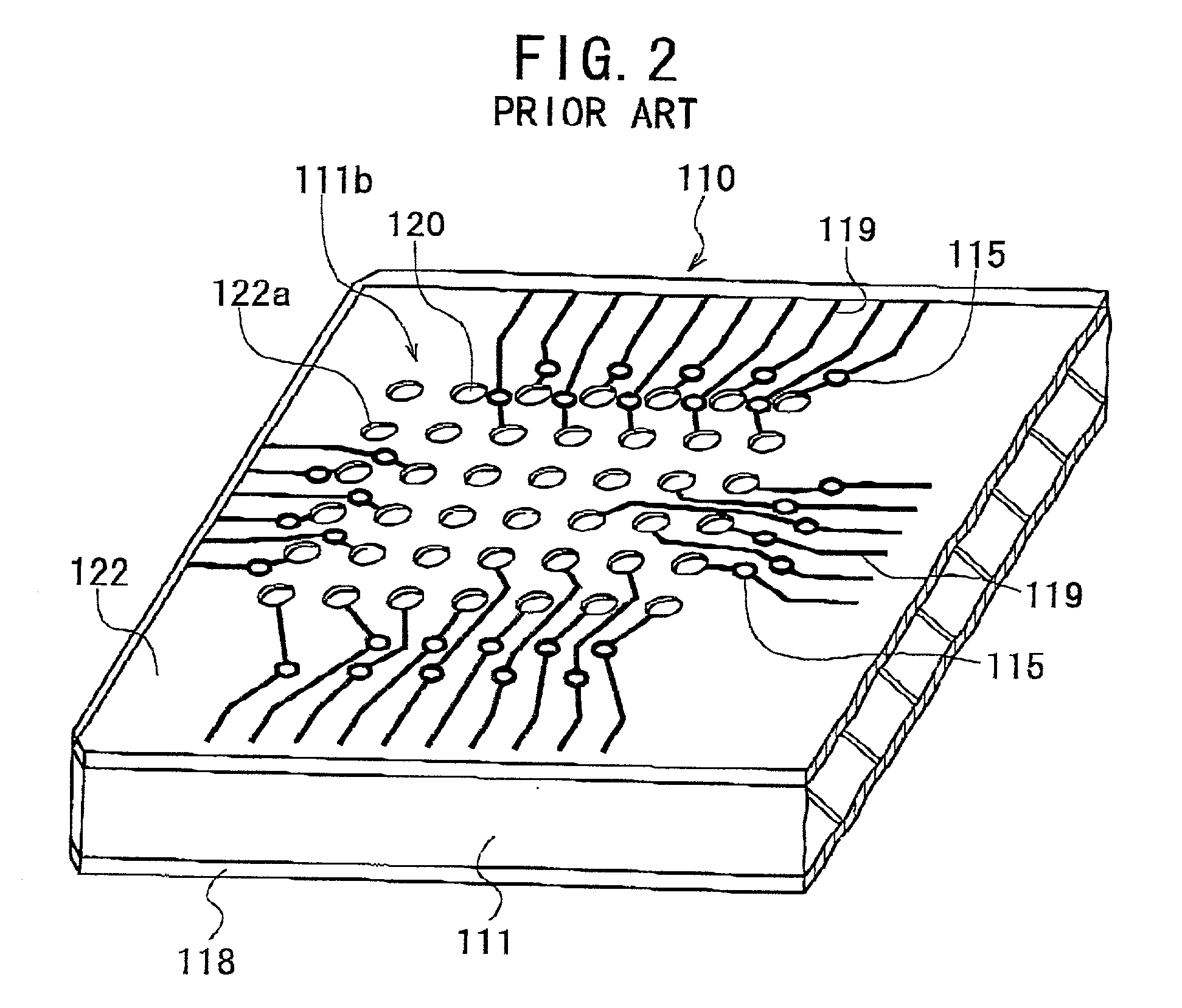
[0104] As shown in FIGS. 3 to 6, the substrate 10 according to the first embodiment comprises a rectangular plate-shaped, rigid dielectric core material 11 having an upper surface and a lower surface. As seen from FIGS. 5 and 6, the core material 11 is strip-shaped and has four mounting areas 11a on its upper surface and four land areas 11b on its lower surface. The areas 11a and 11b are arranged at equal intervals along the longitudinal axis of the care material 11. The core material 11 is typically made of a proper dielectric material, such as woven glass cloth impregnated with epoxy resin.

[0105] A semiconductor element or an IC chip 23 is mounted in each mounting area 11a in a later process, as shown in FIGS. 7 and 8. Lands 20 as external terminals are arranged in the form of array in each land area 11b, as shown in FIG. 4.

[0106] A patterned conductive layer is formed on the upper su...

second embodiment

[0128] FIG. 10 shows the configuration of a semiconductor substrate 10A according to a second embodiment of the invention.

[0129] In the above-described substrate 10 according to the first embodiment, the solder resist layer 18 does not cover the mounting areas 11a of the core material 11 in which the semiconductor elements 23 are respectively mounted. However, the invention is not limited to this structure. It is needless to say the solder resist layer 18 is formed to cover each mounting area 11a, as shown by the substrate 11A of the second embodiment.

[0130] As shown in FIG. 10, the substrate 10A comprises the same configuration as the substrate 10 of the first embodiment as shown in FIGS. 3 to 6, except that additional inner wiring lines 13a are provided, and that windows 26a and 26b are provided in the solder resist layer 18. Therefore, the detailed description about the same configuration is omitted here for the sake of simplification of description by attaching the same referenc...

third embodiment

[0136] FIG. 11 shows the configuration of a semiconductor substrate 10B according to a third embodiment of the invention. In this embodiment, the upper and lower contact areas 11c and 11d provided in the first and second embodiments are eliminated and thus, no part protruding laterally from the solder resist layers 18 and 22. Instead, plated "dummy" through holes 27 are formed on the side face 11e of the core material 11. The side face 11a serves as a contact area. Unlike the first and second embodiments, the width of the solder resist layers 18 and 22 are equal to that of the core material 11. The other configuration is the same as the substrate 10 according to the first embodiment.

[0137] The holes 27, which have the same semicircular cross section, are formed on the vertical side face 11e of the core material 11. Part of the inner wiring lines 13 on the upper surface of the core material 11 are mechanically and electrically connected to the inner wiring lines 21 on the lower surfa...


PUM


Abstract

A substrate for a semiconductor device is provided, which prevents a semiconductor element or IC chip mounted thereon from being broken or damaged electrostatically in a fabrication process sequence or a semiconductor device. The substrate comprises (a) a dielectric core material with an upper surface and a lower surface; the core having a mounting area on the upper surface, a semiconductor element being mounted in the mounting area; the core having a contact area, (b) inner terminals formed on the core material; the inner terminals being used for electrical connection to the semiconductor element mounted on the core material; (c) external terminals formed on the core material; the external terminals being used for electrical connection to an external circuit provided outside the substrate; and (d) inner wiring lines formed on the core material; the inner wiring lines connecting electrically and mechanically the inner terminals with the respective external terminals; part of the inner wiring lines being located in the contact area of the core in such a way as to be able to contact an external conductor provided outside the substrate.

Description

[0001] 1. Field of the Invention[0002] The present invention relates to a substrate for a semiconductor device and a method of fabricating a semiconductor device comprising the substrate and a semiconductor element or an integrated circuit (IC) chip mounted thereon. More particularly, the invention relates to a substrate comprising a dielectric base material (or, a dielectric core), inner terminals for electrical connection to the semiconductor element or chip, an inner circuit electrically connected to the inner terminals, and external terminals electrically connected to the inner circuit for electrical connection to an external circuit provided outside the substrate, and a method of fabricating a semiconductor device using the substrate.[0003] 2. Description of the Related Art[0004] In recent years, there has been the increasing need to mount a semiconductor element or IC chip and its relating electronic components on a substrate at higher density. To meet this need, the Ball Grid...

Claims


Application Information

Patent Timeline
IPC IPC(8): H01L23/12H01L23/31H01L23/48H01L23/498H01L23/60
CPCH01L23/3107H01L23/49805H01L23/60H01L2224/32225H01L2224/48091H01L2224/48227H01L2224/73265H01L2924/15153H01L2924/1517H01L2924/15173H01L2924/00014H01L2924/00012H01L24/48H01L24/45H01L24/49H01L24/73H01L2224/05554H01L2224/451H01L2224/49171H01L2924/14H01L2924/181H01L2924/00015H01L2224/05599H01L2924/00H01L23/48
Inventor ISHIHARA, KAORUSAKOTA, HIROMICHI
Owner NEC ELECTRONICS CORP
Why Eureka
Try Eureka