Image detector having photoconductive layer, linear electrodes transparent to reading light, and signal-readout electrodes shaded from reading light

a photoconductive layer and image detector technology, applied in the field of image detectors, can solve the problems of increasing manufacturing costs, insufficient reading light entering the reading-side photoconductive layer, and increasing manufacturing costs

Inactive Publication Date: 2001-10-04
FUJIFILM CORP +1
View PDF0 Cites 16 Cited by
  • Summary
  • Abstract
  • Description
  • Claims
  • Application Information

AI Technical Summary

Problems solved by technology

Furthermore, when the transmittance of the reading light through the light-entrance electrodes is small, the amount of the reading light entering the reading-side photoconductive layer becomes insufficient.
However, in this case, the manufacturing process becomes more complex, and the manufacturing cost increases.
Therefor

Method used


Image

  • Image detector having photoconductive layer, linear electrodes transparent to reading light, and signal-readout electrodes shaded from reading light
  • Image detector having photoconductive layer, linear electrodes transparent to reading light, and signal-readout electrodes shaded from reading light

Examples


first embodiment

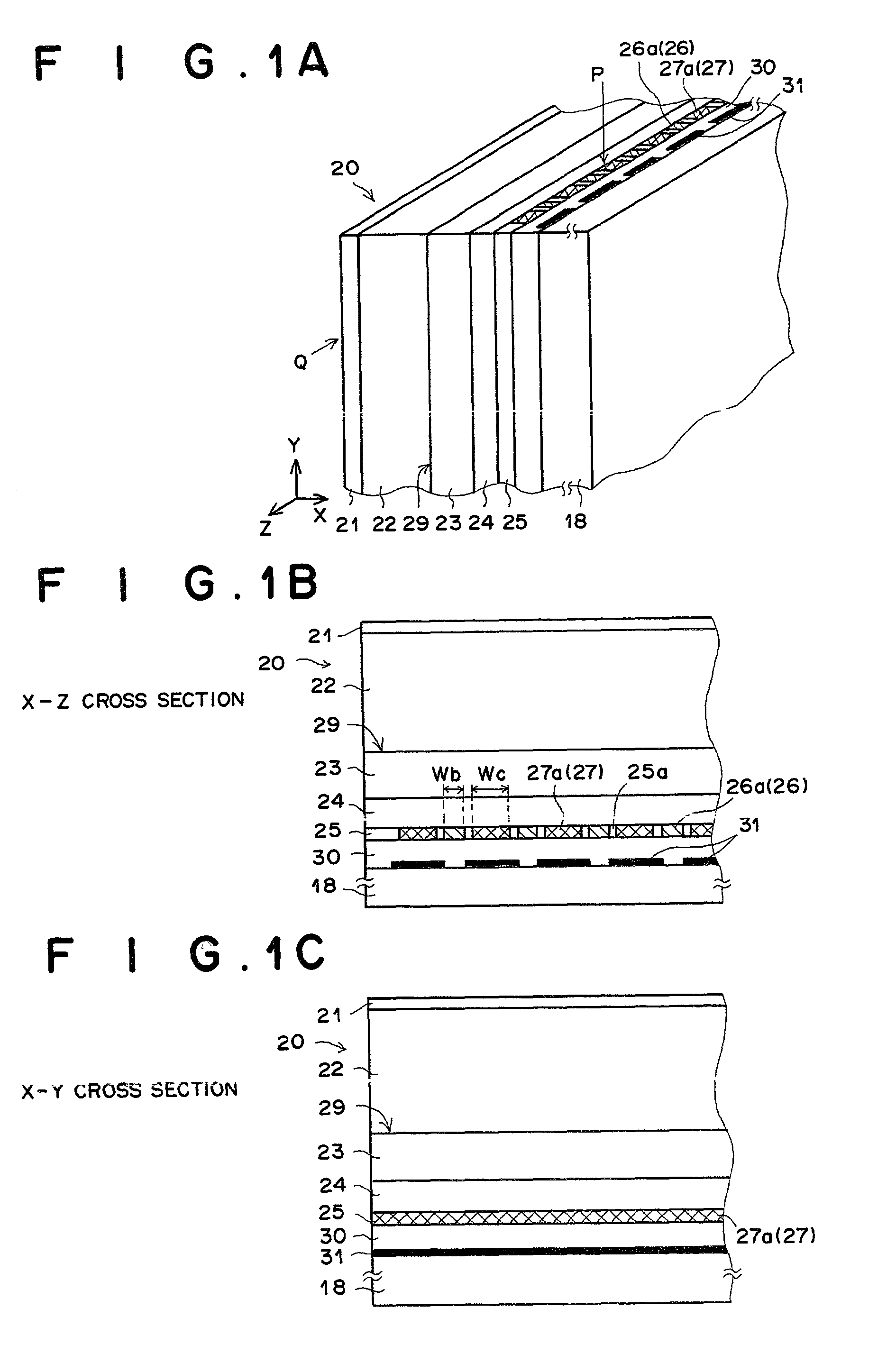
[0046] FIG. 1A a perspective view of a portion of a solid-state radiographic image detector as the first embodiment of the present invention, FIG. 1B illustrates an X-Z cross section of the portion of the solid-state radiographic image detector of FIG. 1A at the position indicated by the arrow Q in FIG. 1A, and FIG. 1C illustrates an X-Y cross section at the position of the portion of the solid-state radiographic image detector of FIG. 1A indicated by the arrow P indicated in FIG. 1A.

[0047] The solid-state radiographic image detector 20 illustrated in FIGS. 1A to 1C comprises a recording-side electrode layer 21, a recording-side photoconductive layer 22, a charge transport layer 23, a reading-side photoconductive layer 24, a reading-side electrode layer 25, an insulation layer 30, and a support 18, formed in this order.

[0048] The recording-side electrode layer 21 is transparent to recording light which carries image information. For example, the recording light is realized by X rays...

second embodiment

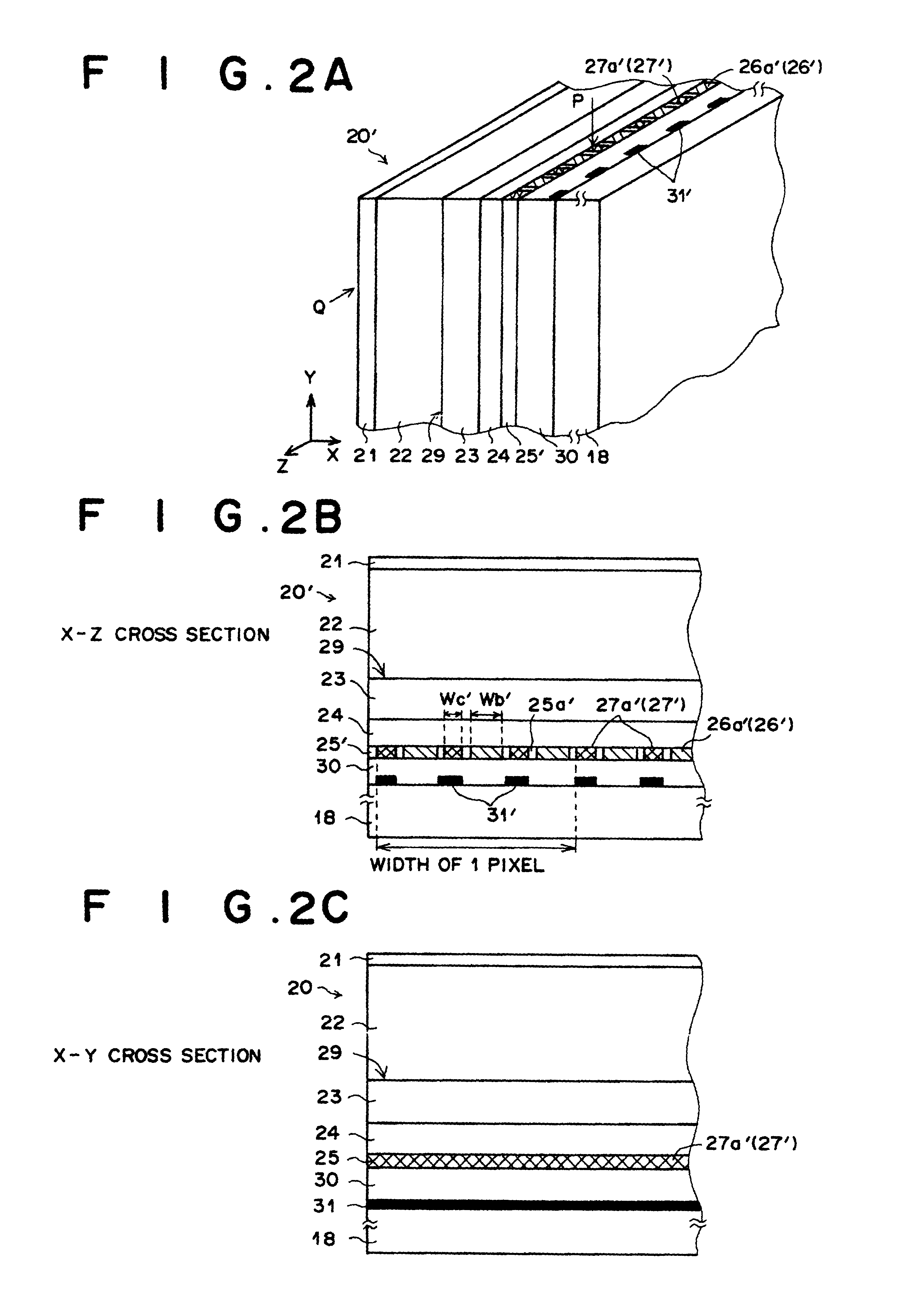
[0080] FIG. 2A is a perspective view of a portion of a solid-state radiographic image detector as the second embodiment of the present invention, FIG. 2B illustrates an X-Z cross section of the portion of the solid-state radiographic image detector of FIG. 2A at the position indicated by the arrow Q in FIG. 2A, and FIG. 2C illustrates an X-Y cross section at the position of the portion of the solid-state radiographic image detector of FIG. 2A indicated by the arrow P indicated in FIG. 2A. The solid-state radiographic image detector 20' illustrated in FIGS. 2A to 2C is identical to the solid-state radiographic image detector 20 illustrated in FIGS. 1A to 1C except for the features explained below. In FIGS. 2A to 2C, elements having the same reference numbers as FIGS. 1A to 1C have the same functions as the corresponding elements in FIGS. 1A to 1C.

[0081] In the solid-state radiographic image detector 20' illustrated in FIGS. 2A to 2C, a plurality of linear electrodes 26a' and a plural...


PUM


Abstract

An image detector includes a recording-side photoconductive layer, a reading-side photoconductive layer, a charge storage region, and a pair of electrode layers. One of the pair of electrode layers located near to the reading-side photoconductive layer comprises a plurality of first linear electrodes transparent to reading light, and a plurality of second linear electrodes each of which corresponds to at least one first linear electrode, and outputs an electric signal corresponding to the amount of latent-image charges when the at least one first linear electrode is scanned with the reading light. The image detector further includes means for making the strength of irradiation of each second linear electrode with the reading light smaller than the strength of irradiation of at least one first linear electrode corresponding to the second linear electrode with the reading light.

Description

[0001] The subject matters disclosed in this specification are related to the subject matters disclosed in the following copending, commonly-assigned U.S. patent applications:[0002] (1) U.S. Ser. No. 09 / 404,371 filed by Shinji Imai on Sep. 24, 1999 and entitled "READ-OUT APPARATUS FOR AN IMAGE DETECTOR," corresponding to Japanese patent application Nos. 10(1998)-271374 and 11(1999)-242876, the latter of which is disclosed in Japanese Unexamined Patent Publication No. 2000-162726;[0003] (2) U.S. Ser. No. 09 / 539,412 filed by Masaharu Ogawa (the inventor of the present application), Shinji Imai, and Toshitaka Agano on Mar. 30, 2000 and entitled "RADIATION SOLID-STATE DETECTORS, AND RADIATION IMAGE RECORD-READING METHOD AND DEVICE USING THE SAME," corresponding to Japanese patent application No. 11(1999)-87922, which is disclosed in Japanese Unexamined Patent Publication No. 2000-284056;[0004] (3) U.S. Ser. No. 09 / 538,479 filed by Shinji Imai on Sep. 24, 1999 and entitled "SOLID-STATE R...

Claims


Application Information

Patent Timeline
IPC IPC(8): G01T1/00G21K4/00G01T1/29G03G17/00H01L27/14H01L31/09H04N5/32
CPCG03G17/00H04N1/00257
Inventor OGAWA, MASAHARU
Owner FUJIFILM CORP
Why Eureka
Try Eureka