Display apparatus

Inactive Publication Date: 2002-02-28
INTELLECTUAL KEYSTONE TECH
View PDF0 Cites 132 Cited by
  • Summary
  • Abstract
  • Description
  • Claims
  • Application Information

AI Technical Summary

Benefits of technology

0018] In accordance with the present invention, since the first TFT and the second TFT are of opposite conduction types, for example, if the first TFT is of an N channel type, the second TFT is of a P channel type, a height of the selecting pulse is to be raised to increase a storage capacity of the first TFT, while the potential of the image signal is to be lowered to reduce the "on" resistance of the second TFT and to increase an emitting luminance. These optimizations in the scanning signal and the image signal are effective at shifting the gate voltage of the first TFT to the direction of increasing the "on" current of this TFT in accordance with that of the image signals, which is at the level to turn the luminescent element "on" state, are written into the holding capacitor, during the selection of the pixel. Therefore, the image signal can be written into the holding capacitor smoothly from the data line through the first TFT. The gate voltage of the first TFT in the event of selecting the pixel corresponds to the potential difference between the scanning signal at the higher potential side and the potential-holding electrode at the time of "on"(the potential of the image signal to turn "on", the potential of the holding capacitor or the gate electrode potential of the second TFT). The gate voltage of the second TFT corresponds to the potential difference between the potential-holding electrode at the time of "on" and the common power supply line. When using the potential of the potential-holding electrode at the time as a reference, the potential of the scanning signal at the higher potential side and the common power supply line are the same in polarity. If the potential of the potential-holding electrode at the time of "on" (the potential of the image signal to turn "on") is changed, both gate voltages of the first TFT and the second TFT change correspondingly, in the same direction and by the same amount. Therefore, a speed up of the display operation can be accomplished, provided that the image signal potential to turn "on" is changed to decrease the resistance of the first TFT at the time of "on". At this time, since the potential of the image signal to turn "on" is changed in the direction that the resistance of the first TFT at the time of "on" is reduced, as a result, a display luminance can be improved. Thus the reduction in the driving voltage and improvement in the display quality can be accomplished simultaneously.
0019] In accordance with the present invention, it is preferable that the gate voltage applied to the second TF

Problems solved by technology

That is, when the pixel is turned "off", the gate voltage (the image

Method used


Image

  • Display apparatus
  • Display apparatus
  • Display apparatus

Examples


Example

[0113] [Embodiment 1 for Carrying Out the Invention]

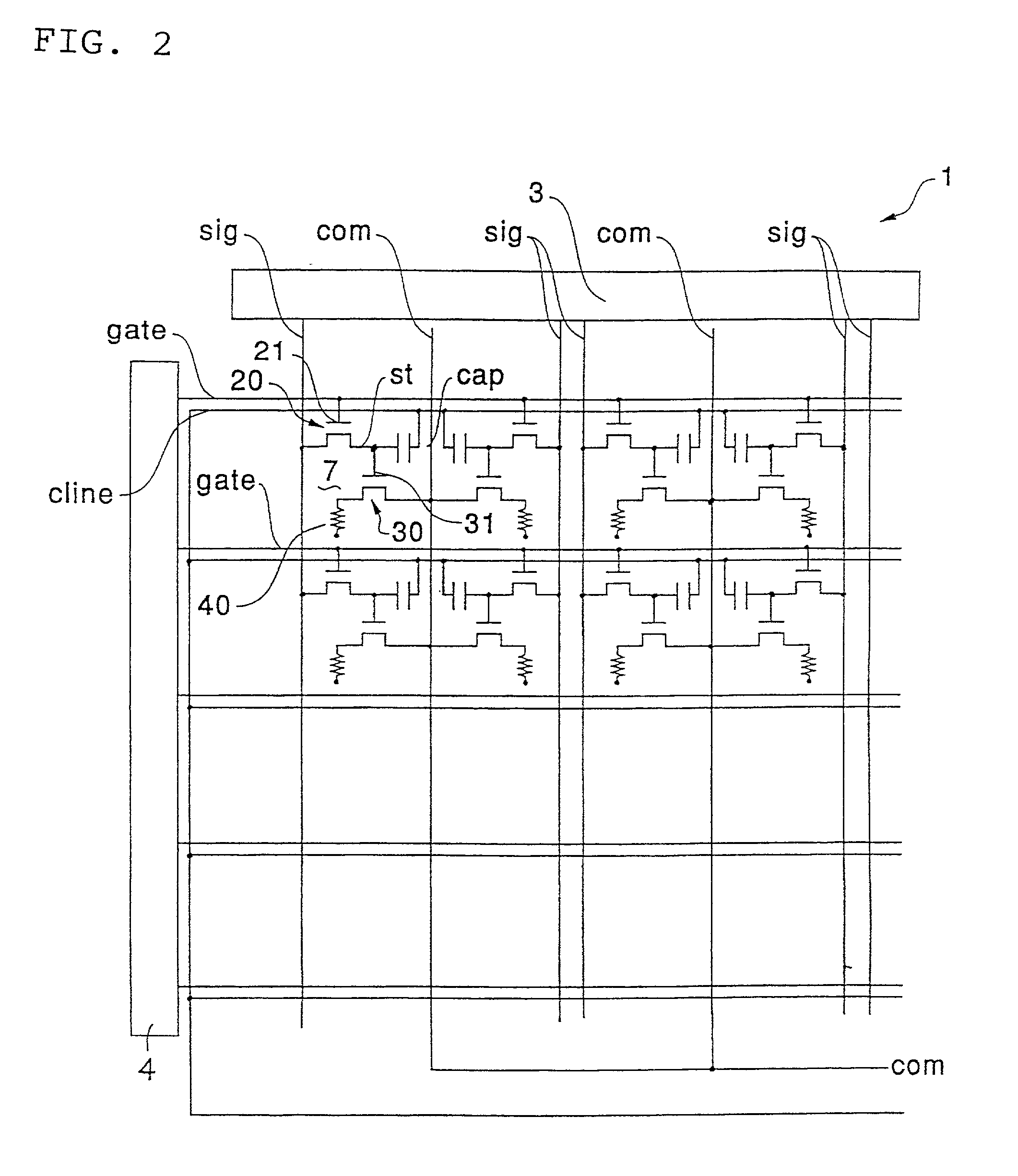
[0114] FIG. 15 is an equivalent circuit diagram showing the pixel structure in the display apparatus 1 in this embodiment. FIGS. 16(A) and (B) are a schematic representation showing electrical connections of each element formed in each pixel, and a wave form chart showing potential changes of driving signals and the like respectively.

[0115] In this embodiment, as shown in FIG. 15 and FIGS. 16 (A) and (B), the first TFT 20 is of an N channel type. Accordingly, when the potential of the scanning signal "S gate" supplied from the scanning line "gate" becomes high, the first TFT 20 turns "on", and the image signal "data" is written into the holding capacitor "cap" from the data line "sig" through the first TFT 20. On the other hand, the potential of the scanning signal "Sgate" supplied from the scanning line "gate" is low, the second TFT is driven and controlled by the image signal "data" held by the holding capacitor "cap".

[0116] In t...

Example

[0130] [Embodiment 2 for Carrying Out the Invention]

[0131] FIG. 19 is an equivalent circuit diagram showing the pixel structure in the display apparatus 1 of this embodiment. FIGS. 20(A) and (B) are a schematic representation showing electrical connections of each element formed in each pixel, and a wave form chart showing potential changes in the driving signal and the like, respectively. In this embodiment, as shown in FIG. 19 and FIGS. 20(A) and (B), the first TFT is formed with an N channel type and the second TFT is formed with a P channel type. Since the second TFT 20 is of a P channel type, from the data line "sig", the image signal "data" in the lower potential side is written into the holding capacitor "cap" of the pixel to be turned "on". The image signal "data" in the higher potential side is written into the holding capacitor "cap" of the pixel to be turned "off". The gate voltage "V gcur" of the second TFT 30 corresponds to the potential difference between the potential...

Example

[0147] [Embodiment 3 for Carrying Out the Invention]

[0148] As shown in the FIG. 23 illustrating an equivalent circuit diagram, this embodiment is an example of structures where the first TFT 20 is of an N channel type and the second TFT 30 is of a P channel type in any pixel 7 the same as Embodiment 2. In the display apparatus 1 according to this embodiment, the potential of the common power supply line "com" is set higher than the potential of the opposite electrode "op" of the luminescent element 40 because the second TFT 30 is of a P channel type. When the second TFT 30 is turned "on", the current flows from the common power supply line "com" to the luminescent element 40, as illustrated by the arrow "E". Since this embodiment is similar to Embodiment 2, only the differences will be described, and the things in common will be omitted. This embodiment is different from Embodiment 2 in that the holding capacitor "cap" is omitted. By this structure, the potential changes of the pote...


PUM


Abstract

A display apparatus, that includes current driving type luminescent elements, has a driving system that takes the conduction types of TFTs to control the emission of the luminescent elements into consideration. In order to reduce driving voltage and improve display quality simultaneously, the arrangement is provided such that if the second TFT (30) which performs the "on-off" function of the current for the luminescent element (40) is of an N channel type, the potential of the common power supply line ("com") is lowered below the potential of the opposite electrode ("op") of the luminescent element (40) to obtain a higher gate voltage ("Vgcur"). In this case, if the first TFT (20) connected to the gate of the second TFT (30) is of a P channel type, when using the potential of the potential-holding electrode ("st") at the "on" state as a reference, potentials of the scanning signal ("Sgate") at the lower potential and the common power supply line ("com") are rendered of the same polarities with respect to this potential of the potential-holding electrode ("st"). Therefore, the potential of the image signal ("data") to turn "on" can be shifted within the range of the driving voltage in the display apparatus (1) in the direction to reduce resistances at the "on" states of the first TFT (20) and the second TFT (30) to reduce driving voltage and improve display quality.

Description

[0001] The present invention relates to an active matrix type display apparatus including luminescent elements such as EL (Electro-luminescence) elements or LED (Light Emitting Diode) elements which emit light by driving current flowing in thin films of organic semiconductors or the like, and also including thin film transistors (hereinafter TFT's) to control the emitting operation of these luminescent elements. More particularly, the present invention relates to a technique of driving each element formed in this type of display apparatus.[0002] Active matrix type display apparatuses incorporating luminescent elements of a current controlling type, such as EL elements and LED elements, have been proposed. Since any luminescent element employed in this type of display apparatus emits by itself, there are advantages in using no back-light and in having a minimal dependence on the viewing angle and the like.[0003] FIG. 31 is a block diagram illustrating an active matrix type display ap...

Claims


Application Information

Patent Timeline
IPC IPC(8): G09G3/00G09G3/32H01L27/32H01L33/08H01L33/26H01L33/42H01L51/52H05B44/00
CPCG09G3/006H01L2251/5315G09G3/3258G09G3/3266G09G2300/0408G09G2300/0417G09G2300/0426G09G2300/0439G09G2300/0465G09G2300/08G09G2300/0809G09G2300/0842G09G2300/0847G09G2300/0876G09G2310/0254G09G2310/0256G09G2310/0262G09G2310/0283G09G2310/06G09G2320/043G09G2330/021H01L27/3244H01L27/3246H01L27/3262H01L27/3276H01L51/0005H01L51/5206H01L51/5221H01L51/5234H01L51/5281H01L51/5284G09G3/3233H10K59/122H10K59/12H10K59/1213H10K59/131H10K71/135H10K50/81H10K50/828H10K50/86H10K50/865H10K2102/3026G09G3/30
Inventor OZAWA, TOKUROHKIMURA, MUTSUMI
Owner INTELLECTUAL KEYSTONE TECH
Why Eureka
Try Eureka