Semiconductor device

a technology of semiconductor devices and diodes, applied in semiconductor devices, semiconductor/solid-state device details, electrical apparatus, etc., can solve the problems of low current drivability, delay in turn-on operation, and diode resistance reduction

Inactive Publication Date: 2002-03-21
RENESAS ELECTRONICS CORP
View PDF0 Cites 14 Cited by
  • Summary
  • Abstract
  • Description
  • Claims
  • Application Information

AI Technical Summary

Problems solved by technology

Thus, the limited thickness of the SOI layer 350 causes problems of low current drivability and a delay in turn-on operation.
This reduces the resistance

Method used


Image

  • Semiconductor device
  • Semiconductor device
  • Semiconductor device

Examples


Embodiment Construction

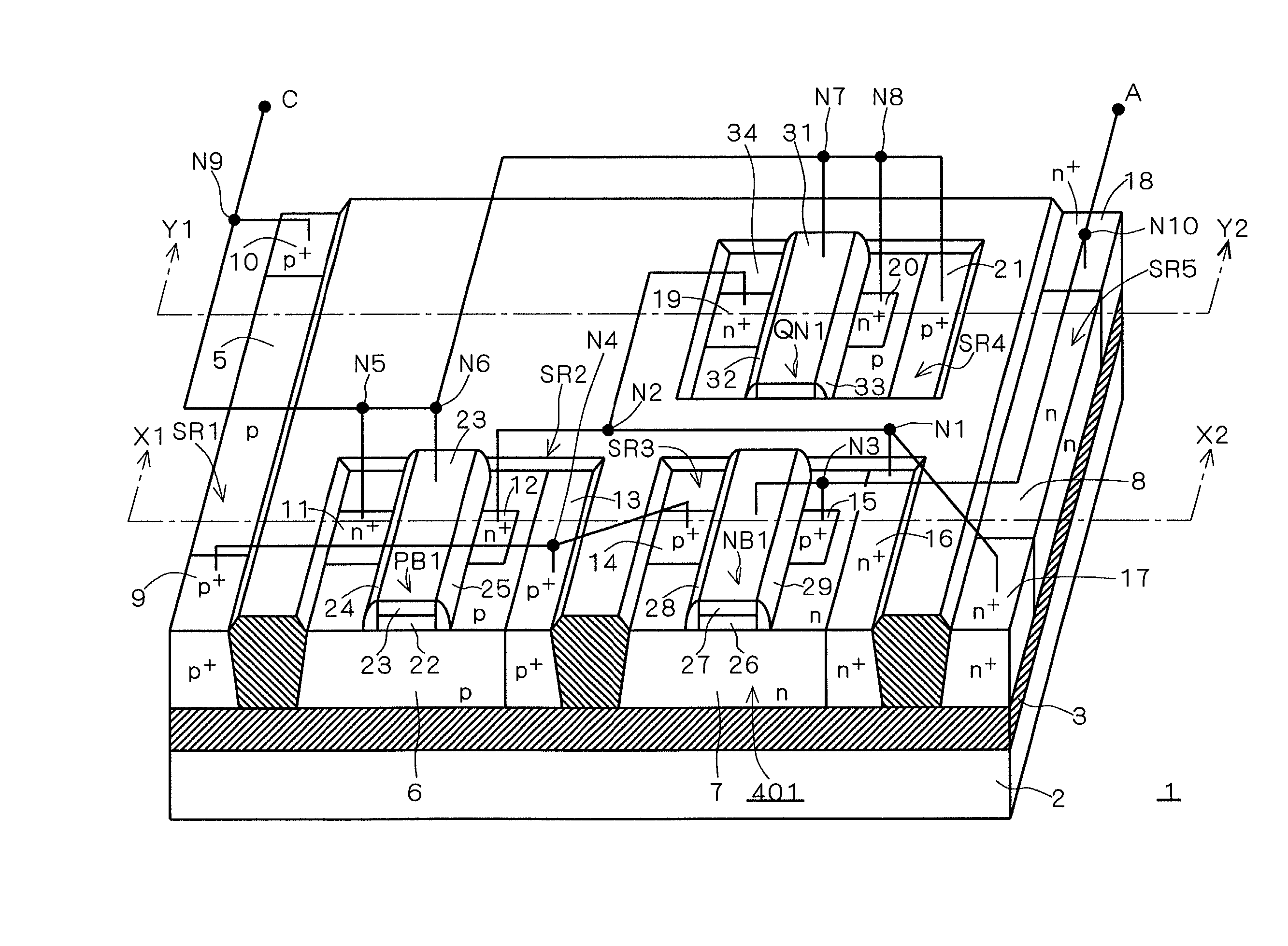
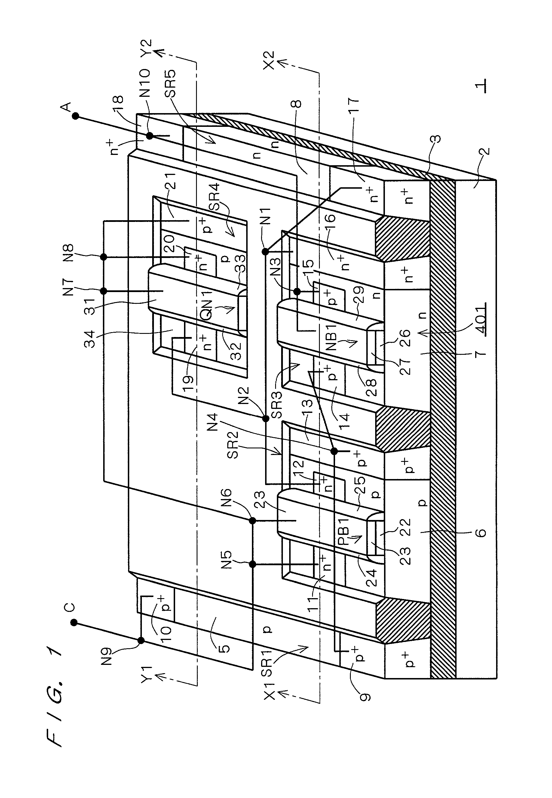
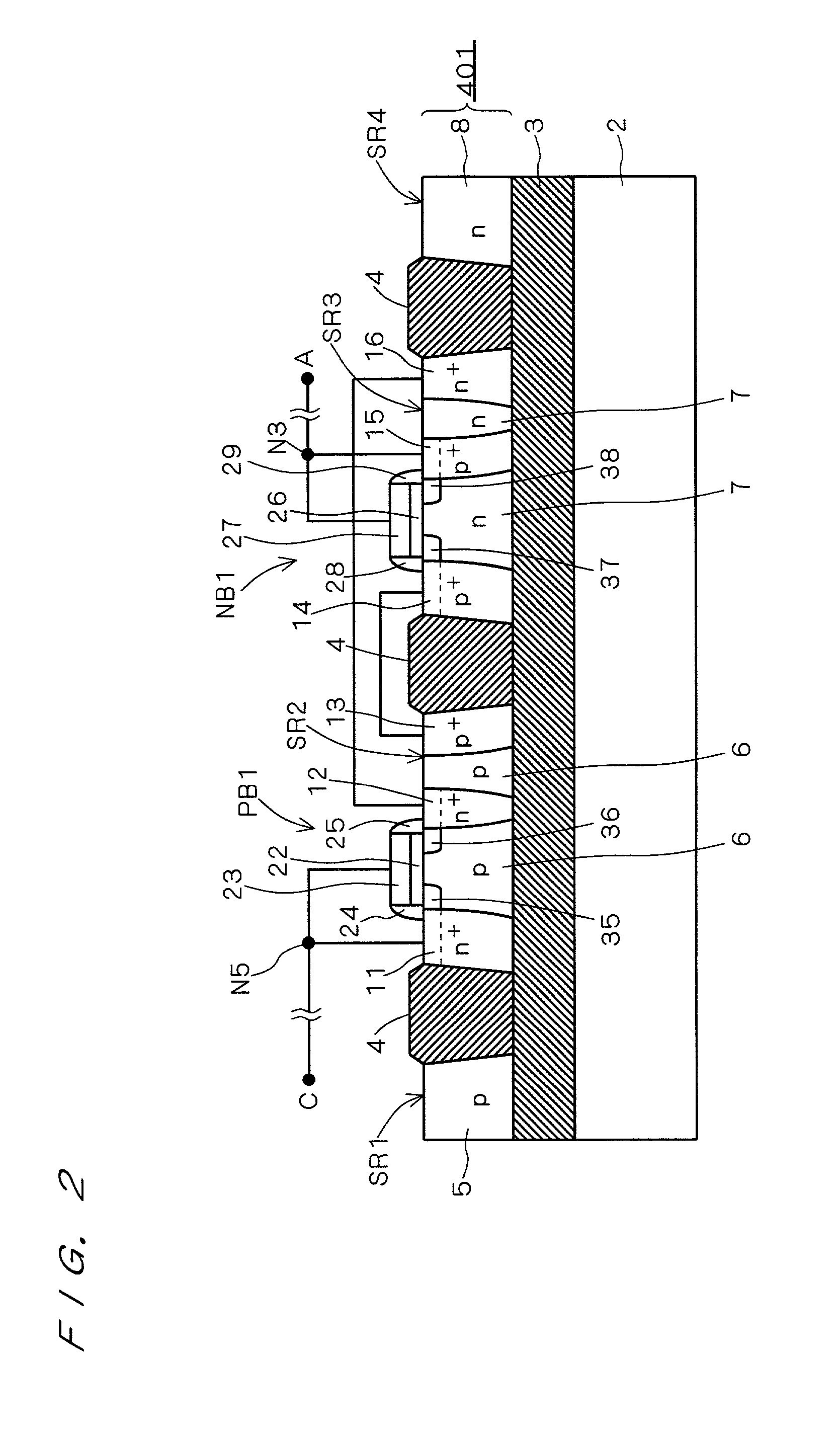
to Bipolar Transistor The aforementioned metal silicide film is also applicable to the bipolar transistors PB1 and NB1. FIG. 25 is a cross-sectional view illustrating such an example, taken along the section line X1-X2 of FIG. 1. As shown in FIG. 25, a metal silicide film 190 is formed to cover the main surface of the SOI layer 401 in the element regions SR2 and SR3, and part of the gate. That is, in either of the bipolar transistors PB1 and NB1, the gate and the source (also, the body) are electrically connected by the metal silicide film 192. The gate can thus be short-circuited with the source with low resistance and stability, which suppresses the holding voltage V.sub.H with stability.

[0165] 4. Fourth Preferred Embodiment

[0166] FIG. 26 is a perspective view of a semiconductor device according to a fourth preferred embodiment, when viewed angularly from the above. FIGS. 27, 28, and 29 are cross-sectional views of this semiconductor device 80 of FIG. 26, taken along the section l...


PUM


Abstract

A diode (QN1) is connected in parallel to one of two bipolar transistors (PB1, NB1) constituting a semiconductor-controlled rectifier or SCR (400) in such a direction as to encourage positive feedback. This enhances current drivability and accelerates a turn-on operation.

Description

[0001] 1. Field of the Invention[0002] The present invention relates to a semiconductor device suitable for use as a protection circuit for protecting an integrated circuit against electrostatic discharge (ESD), and in particular to improvements for the purposes of enhancing current drivability and accelerating a turn-on operation.[0003] 2. Description of the Background Art[0004] Conventionally, ESD protection circuits have been utilized for preventing integrated circuits formed in semiconductor substrates from being damaged by the application of a positive or negative high voltage, as overshooting or undershooting input voltage, due to the accumulation of electrostatic charge in the human body or machinery. Semiconductor controlled rectifiers (generally referred to as "SCRs") are a kind of such ESD protection circuits.[0005] FIGS. 42 and 43 are a cross-sectional view and a circuit diagram of a conventional SCR, respectively. This SCR 200 is formed in an SOI substrate including a su...

Claims


Application Information

Patent Timeline
IPC IPC(8): H01L21/822H01L21/76H01L27/02H01L27/04H01L29/786
CPCH01L27/0262H01L2924/0002H01L2924/00H01L27/04
Inventor KUNIKIYO, TATSUYA
Owner RENESAS ELECTRONICS CORP
Why Eureka
Try Eureka