

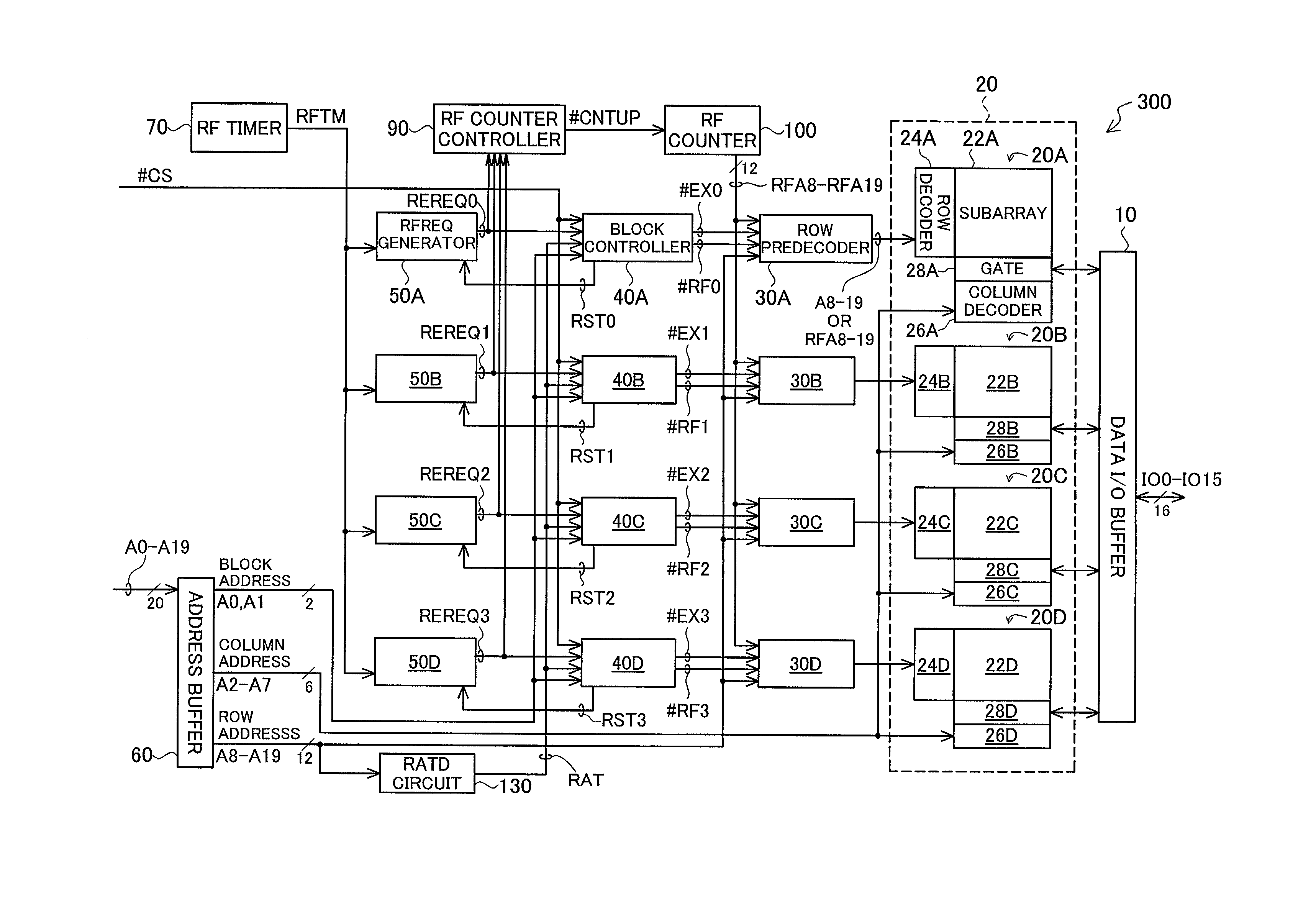
Activation of word lines in semiconductor memory device
a technology of word lines and memory devices, which is applied in the direction of information storage, static storage, digital storage, etc., can solve the problems of wasting power, having a lower capacity than dram, and being more expensiv
- Summary
- Abstract
- Description
- Claims
- Application Information
AI Technical Summary
Benefits of technology
Problems solved by technology
Method used
Image

Examples
Embodiment Construction
in an Electronic Device:
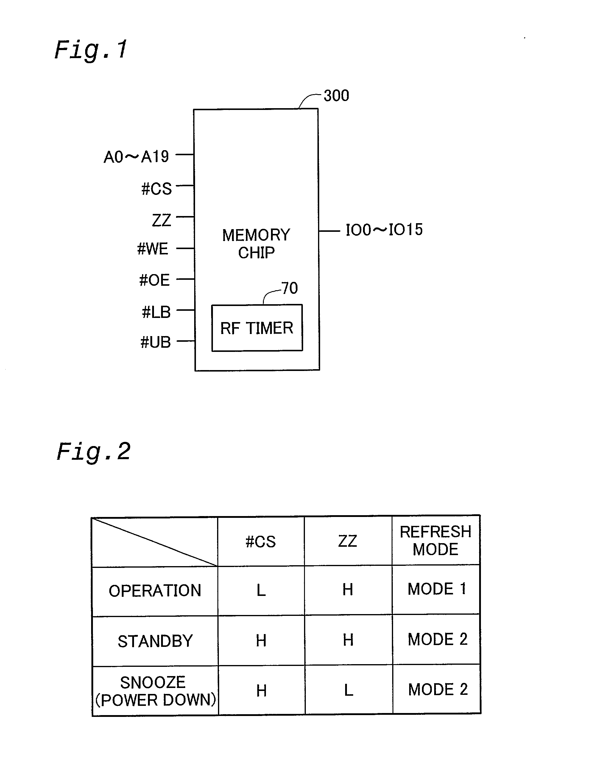
[0209] FIG. 21 is a perspective view of a mobile phone by way of an exemplary electronic device embodying the semiconductor memory device of the present invention. Mobile phone 600 comprises a body 610 and a cover 620. Body 610 is provided with a keyboard 612, a liquid crystal display 614, a receiver 616, and a body antenna 618. Cover 620 is provided with a transmitter 622.
[0210] FIG. 22 is a block diagram showing the electronics of the mobile phone 600 of FIG. 21. CPU 630 is connected via a bus line to keyboard 612; an LCD driver 632 for driving liquid crystal display 614; an SRAM 640, a VSRAM 642; and an EEPROM 644.
[0211] SRAM 640 is used as a high speed cache memory, for example. VRAM 642 is used as a working memory for image processing, for example. Memory chip 300 may be used for VSRAM 642 (referred to as virtual SRAM or pseudo SRAM). EEPROM 644 contains various settings for the mobile phone 600.
[0212] When operation of mobile phone 600 is temporarily su...
PUM
 Abstract
Description
Claims
Application Information